Chapter6 Functions of Combinational Logic
6.1 Adders
The Half Adder(半加器)
The half-adder accepts two binary digits on its inputs and produces two binary digits on outputs, a sum bit and a carry bit.
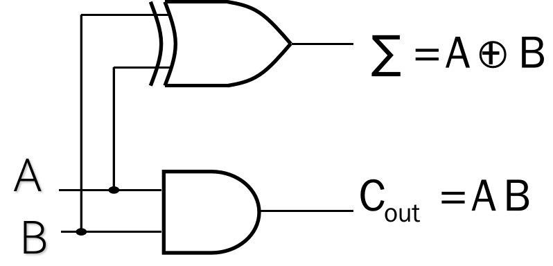
| 输入 A | 输入 B | (Sum) | 进位 (Carry) |
|---|---|---|---|
| 0 | 0 | 0 | 0 |
| 0 | 1 | 1 | 0 |
| 1 | 0 | 1 | 0 |
| 1 | 1 | 0 | 1 |
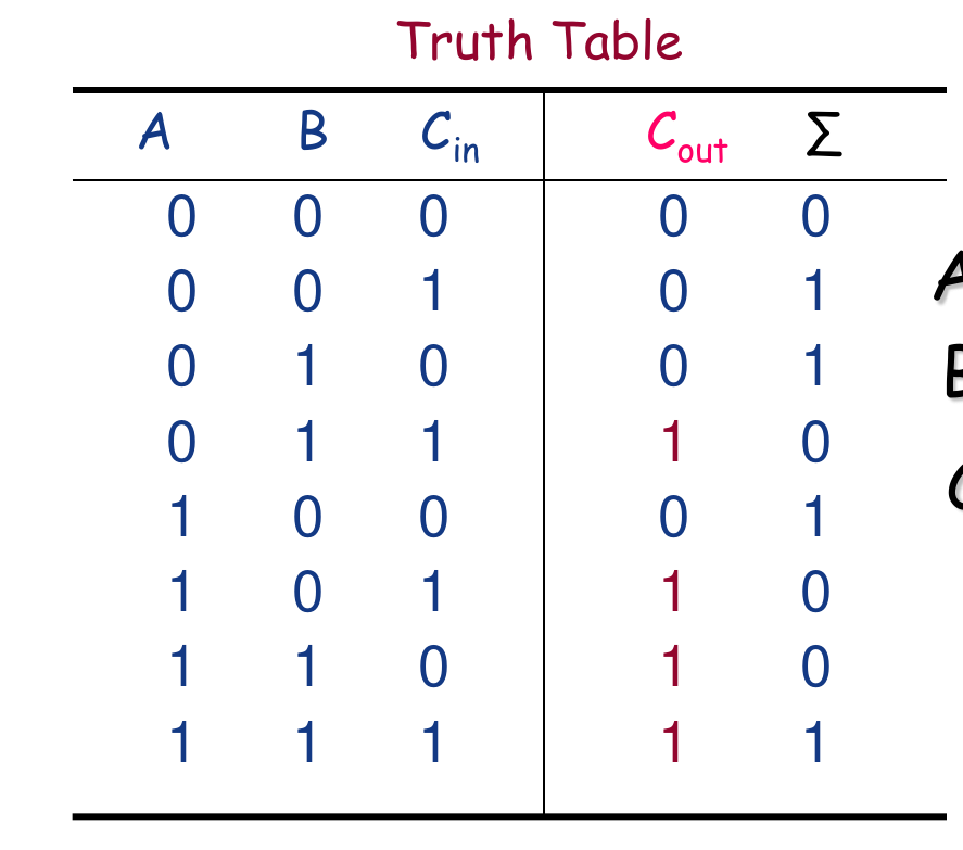
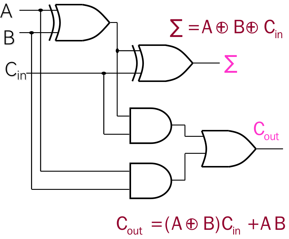
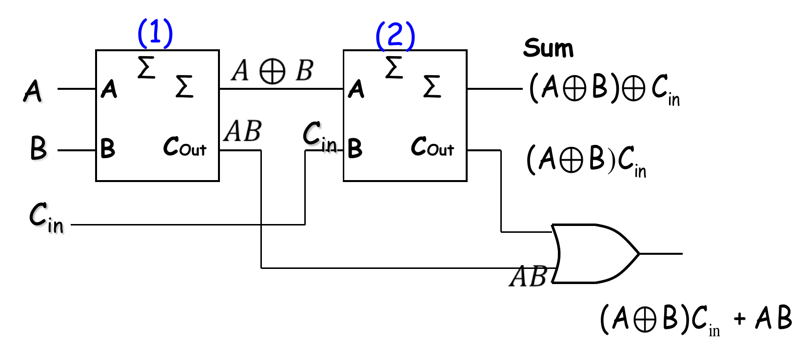
The Full Adder(全加器)
The full-adder accepts two inputs and input carry and generates a sum output and an output carry.
使用逻辑门实现全加器
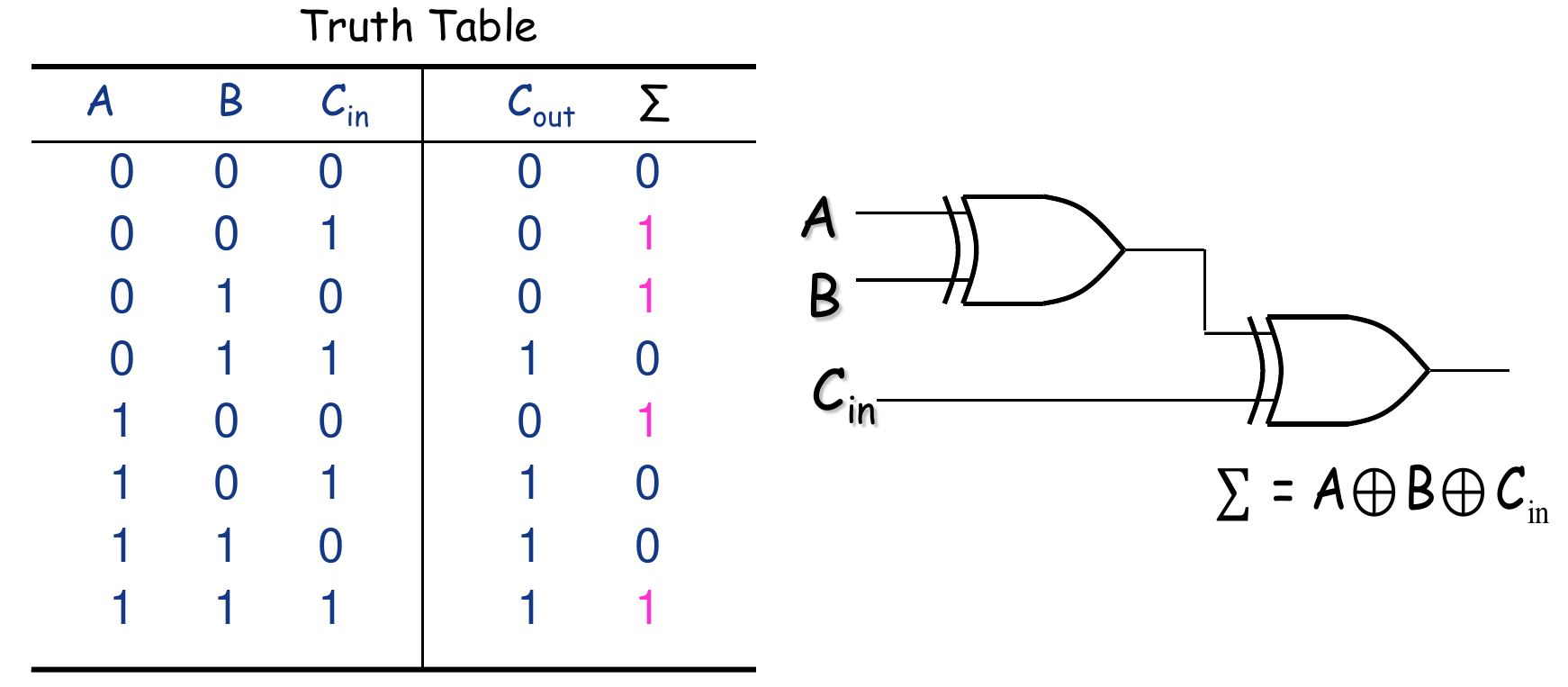 $$
\begin{align}
\sum &= \overline{A}BC_{in} + \overline{A}\overline{B}C_{in} + A\overline{B}\overline{C}_{in} + ABC_{in} \\
&= \overline{A}(BC_{in} + \overline{B}C_{in}) + A(\overline{B}\overline{C}_{in} + BC_{in}) \\
&= \overline{A}(B \oplus C_{in}) + A(\overline{B \oplus C_{in}}) = A\oplus B\oplus C_{in}
\end{align}
$$
$$
\begin{align}
\sum &= \overline{A}BC_{in} + \overline{A}\overline{B}C_{in} + A\overline{B}\overline{C}_{in} + ABC_{in} \\
&= \overline{A}(BC_{in} + \overline{B}C_{in}) + A(\overline{B}\overline{C}_{in} + BC_{in}) \\
&= \overline{A}(B \oplus C_{in}) + A(\overline{B \oplus C_{in}}) = A\oplus B\oplus C_{in}
\end{align}
$$
 $$
C_{out} = \overline{A}BC_{in} + A\overline{B}C_{in} + A\overline{B}\overline{C}_{in} + ABC_{in}
= (\overline{A}B + A\overline{B})C_{in} + AB
= (A \oplus B)C_{in} + AB
$$
**总结**
$$
\begin{cases}
\sum = A\oplus B\oplus C_{in} \\
C_{out} = (A \oplus B)C_{in} + AB
\end{cases}
$$
$$
C_{out} = \overline{A}BC_{in} + A\overline{B}C_{in} + A\overline{B}\overline{C}_{in} + ABC_{in}
= (\overline{A}B + A\overline{B})C_{in} + AB
= (A \oplus B)C_{in} + AB
$$
**总结**
$$
\begin{cases}
\sum = A\oplus B\oplus C_{in} \\
C_{out} = (A \oplus B)C_{in} + AB
\end{cases}
$$
用两个半加器实现全加器
Parallel Binary Adders
- Two or more full-adders are connected to form parallel binary adders.
- A single full-adder is capable of adding two 1-bit binary numbers and an input carry. To add binary numbers with more than one bit, additional full-adders must be used.
- The carry output of each adder is connected to the carry input of the next higher-order adder.
- In terms of the method used to handle carries in a parallel adder, there are two types: the ripple carry adder and the carry look-ahead adder.
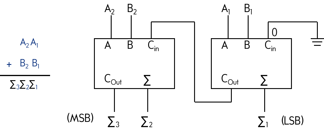
Example: 4-bit parallel adders
A group of four bits is called a nibble(半字节). A basic 4-bit parallel adder is implemented with four full-adders.
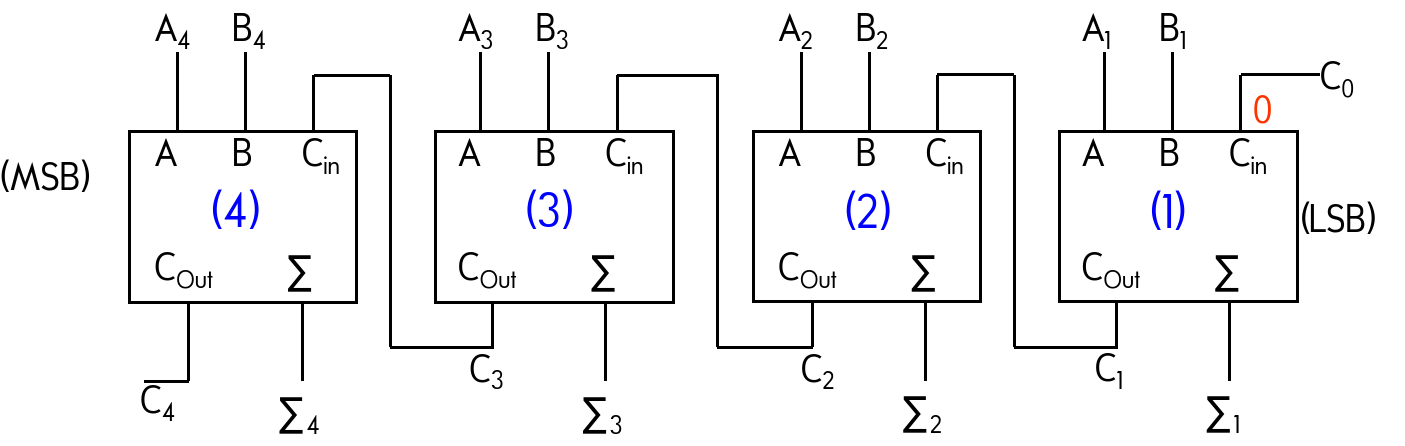
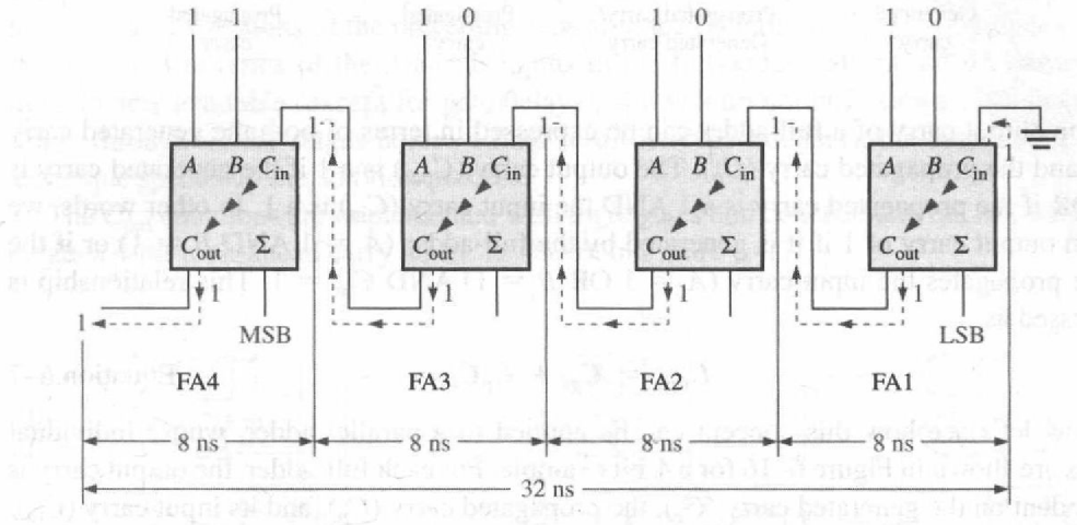
Method 1: Ripple Carry Adder (串行进位加法器) RCA
- Ripple Carry Adder is one in which the carry output of each full-adder is connected to the carry input of the next higher-order stage.
- The sum and the output carry of any stage cannot produced until the input carry occurs; this causes a time delay in the addition process.
- 完整的位串行进位加法器加法需要 的时间
Method 2: Look-Ahead Carry Adder (超前进位加法器) CLA
The look-ahead carry adder anticipates the output carry based on the input bits, and produces the output carry by either carry generation or carry propagation.
- 一个N位的CLA可以在 的时间内计算完N位的加法
- CLA在位数较大的情况下,逻辑电路复杂程度会大幅增加。实际使用的时候,一般不会把一个位数很大的加法器直接以CLA的形式展开,而是以2-bit,4-bit或8-bit的CLA作为一个单元,然后把各个单元作为一个整体再用CLA的方式连起来,这样可以在计算速度和电路复杂度之间做一个权衡。这种结构的总体时间复杂度为
基本定义和概念
- 进位生成 (Carry Generation) : 当输入 和 都为 1 时,无论低位的进位 是多少,本位都会产生一个向高位的进位。
- 进位传播 (Carry Propagation) : 当输入 或 中有一个为 1 时 (即 ),本位会将来自低位的进位 传递到高位。
- 注意:在某些设计中,进位传播也可能定义为 (异或)。PPT中的定义是 (或)。我们将按照PPT中的定义进行推导。
进位项推导
全加器第 位的进位输出 (Carry Out) 取决于两种情况:
- 本位自己产生了进位 ( )。
- 本位将来自低位的进位 (Carry In) 传播了上去 ( 且 )。
所以,第 位的进位输出逻辑表达式为:
使用 和 代替,得到:
这里的 是第 位的进位输入,它实际上就是第 位的进位输出 。所以:
然后进行迭代表达式循环展开,直到表达式中的所有逻辑量都是由输入直接决定的
这里的 是从更低位过来的输入
注意区分题目的最低位是0还是1,这个有些题目可能是不一样的。如果最低位是0的话,那么表达式就变成
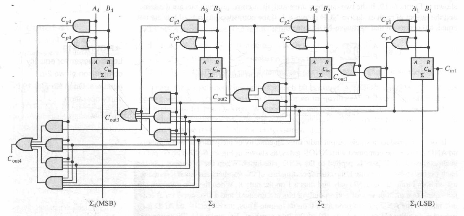
以这个4-bit CLA为例(最低位从1开始):
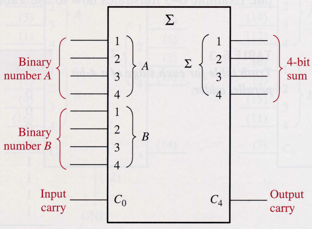
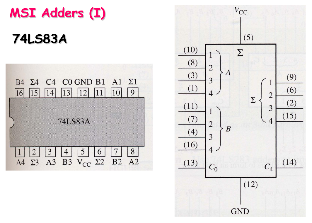
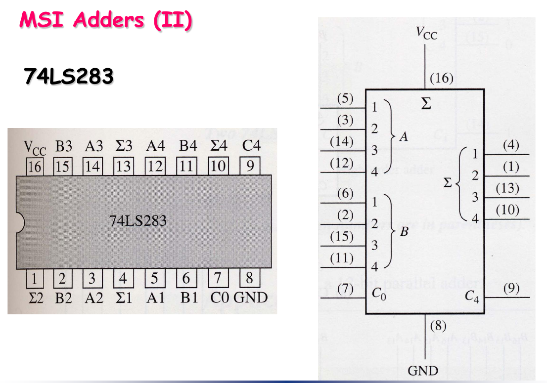
集成的加法器芯片
- 会用就行,知道管脚定义,会识别管脚编号,会连线扩展即可
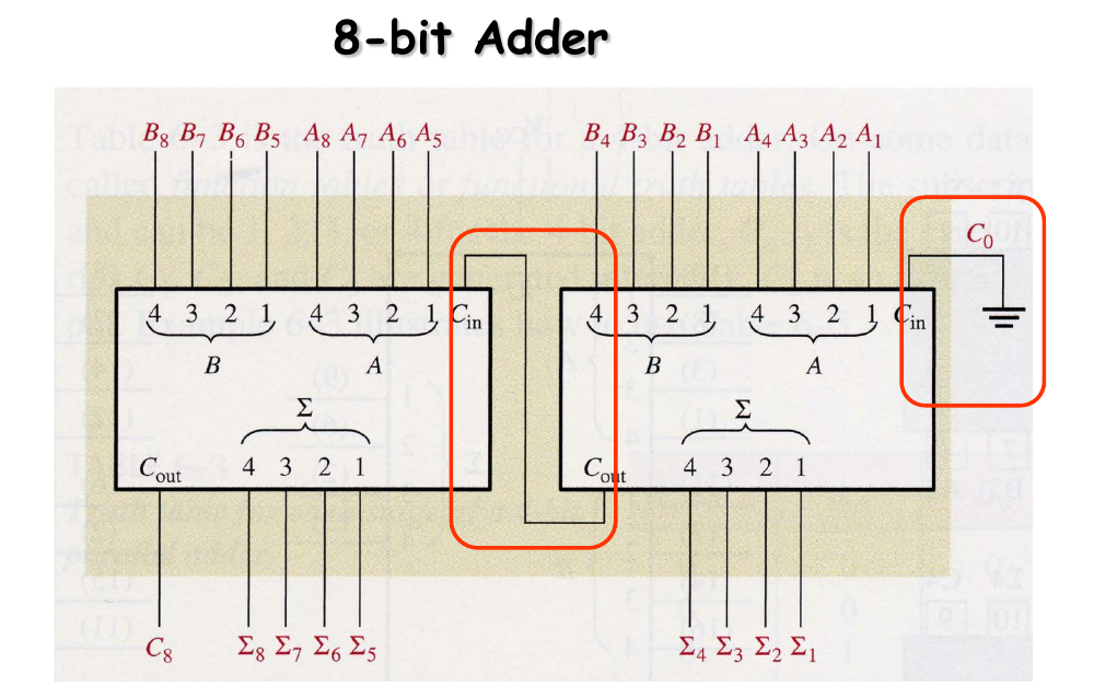
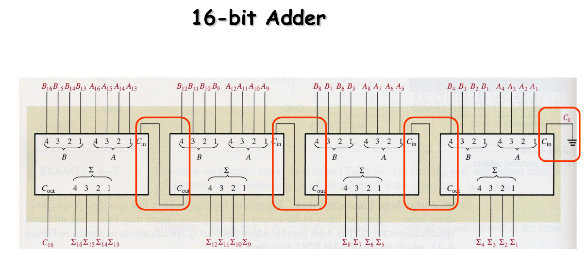
Adders Expansion
6.2 Comparators
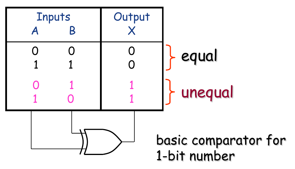
- The basic function of a comparator is to compare the magnitudes of two binary quantities to determine the relationship of those quantities.
- In its simplest form, a comparator determines whether two numbers are equal.
Basic Comparator
1-bit comparator
2-bit comparator
Advanced Comparators
- In addition to the equality output, many comparators provide additional outputs that indicates which of the two numbers is the larger.
- That is, there is an output that indicates when number A is greater than number B (A > B) and an output that indicates when number A is less than number B (A < B).
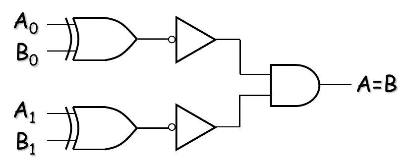
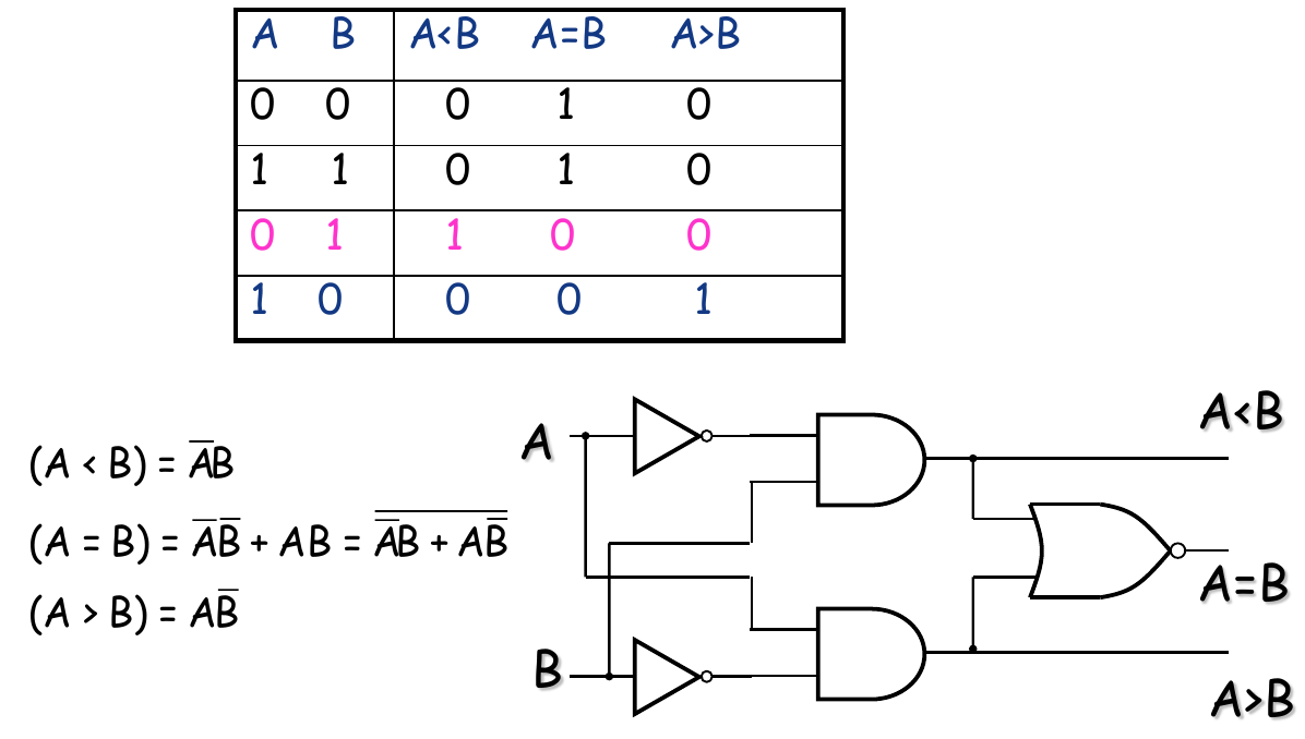
One-bit Comparator
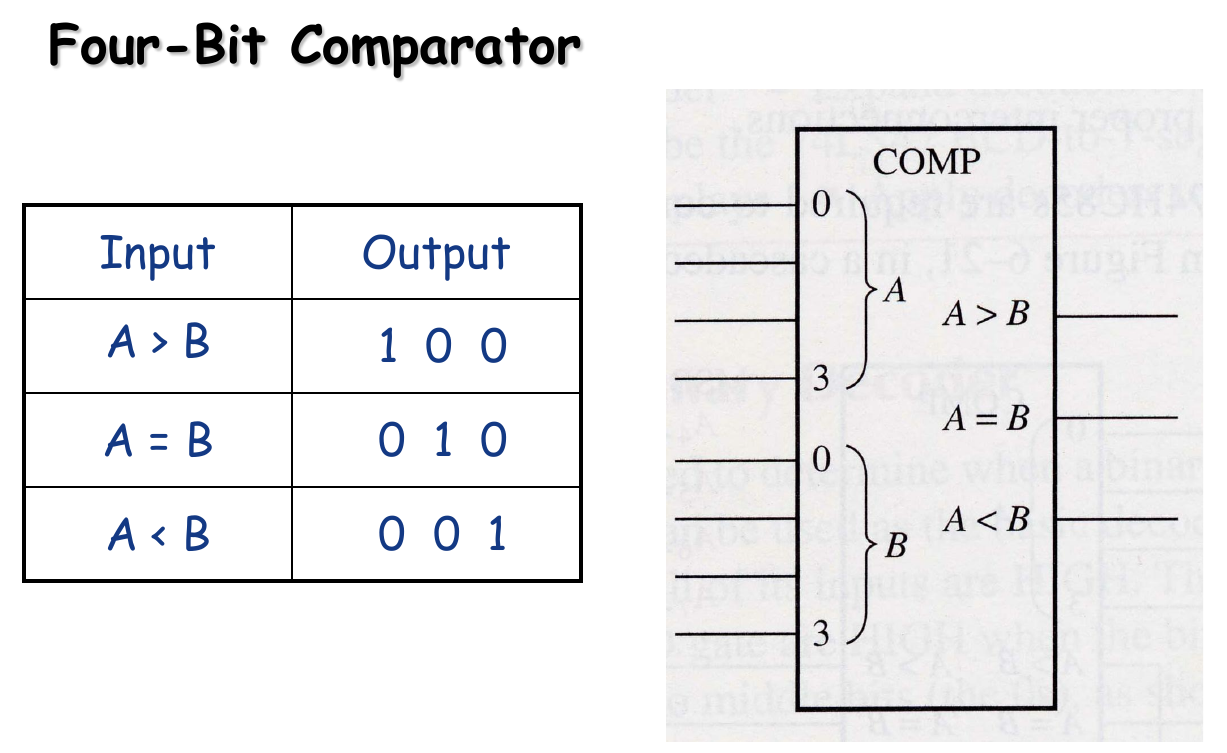
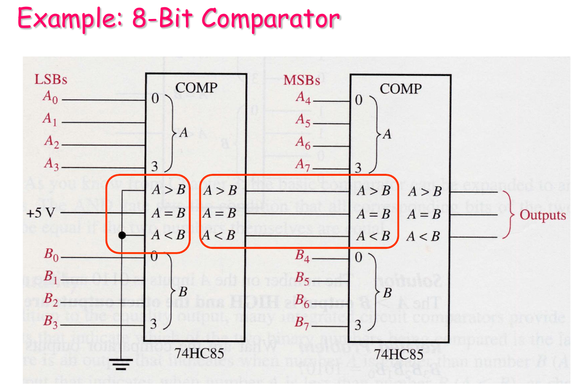
4-bit Comparator
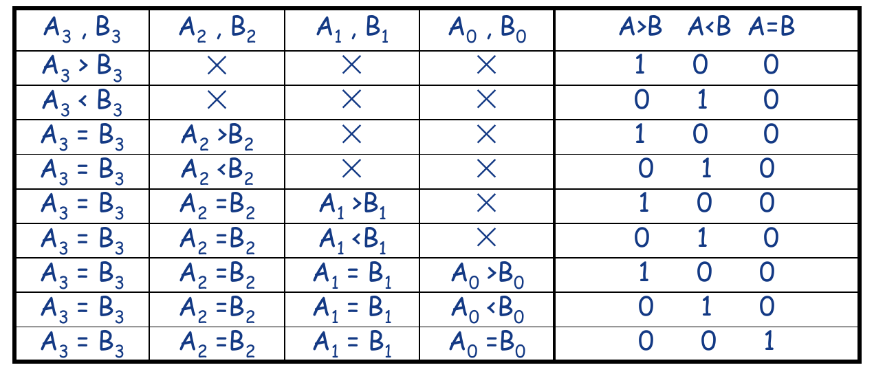
Comparison Rules
- Begin from MSB
- If , then
- If , then
- If , then compare the lower bits
- Repeat this operation to LSB
Bit Comparison Logics
- :
- :
- : or
Truth Table
Logic Expression
Integrated Comparator
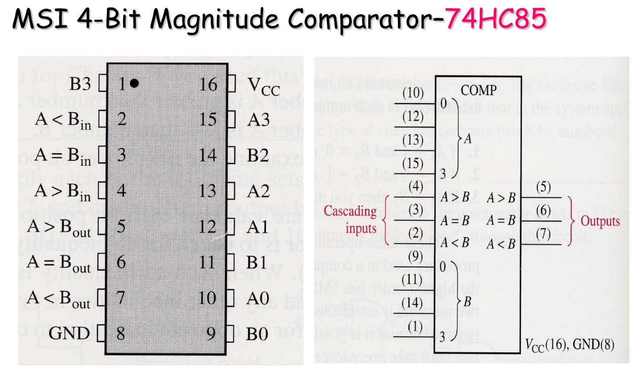
Comparator Expansion
6.3 Decoders
- The Basic function of a decoder is to detect the presence of a specified combination of bits (code) on its inputs and to indicate the presence of that code by a specified output level.
- In its generation form, a decoder has n input lines to handle n bits and from one to output lines to indicate the presence of one or more n-bit combinations.
The Basic Binary Decoder
- Implemented with NOT Gates & AND Gate
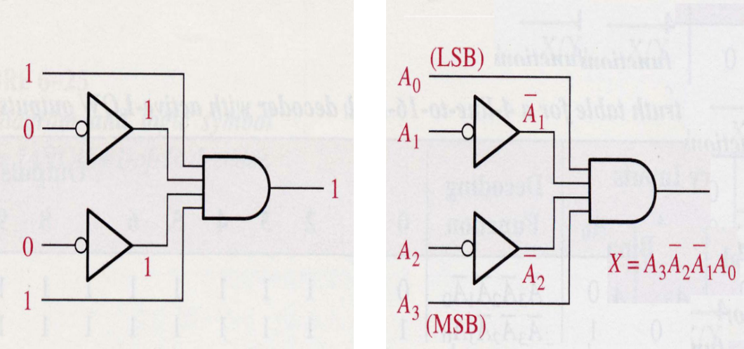
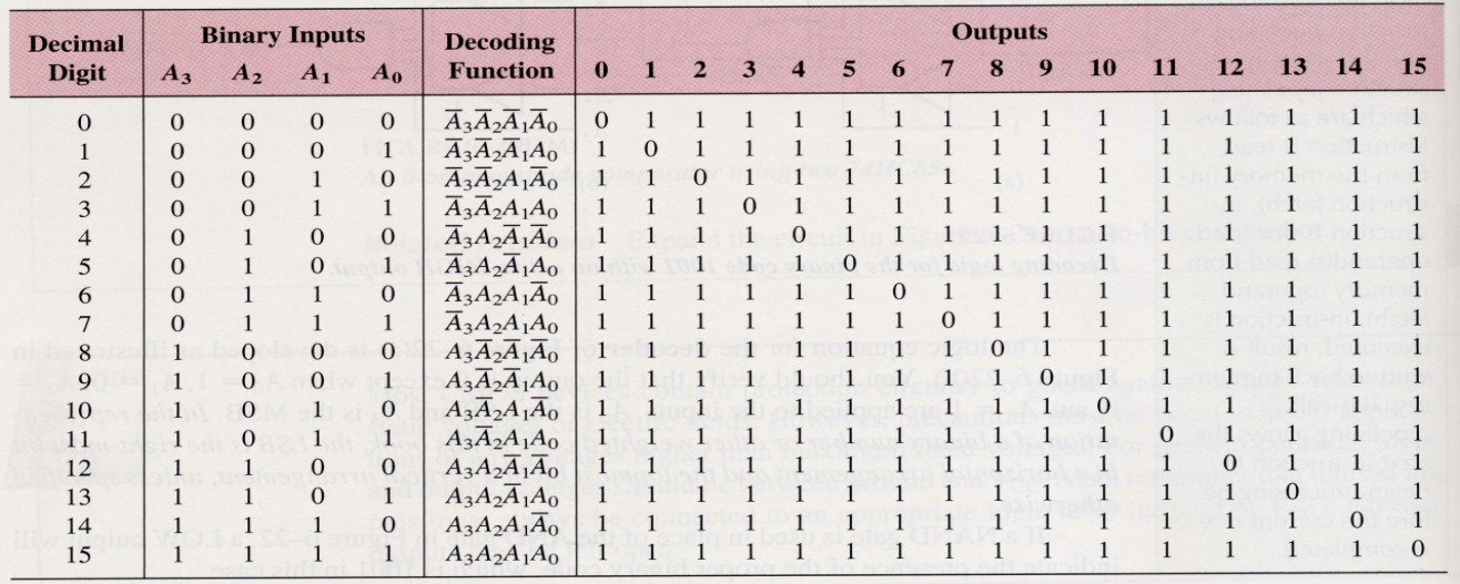
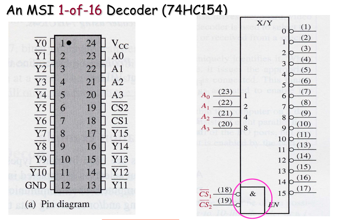
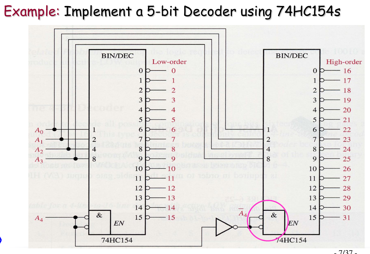
The 4-Bit Decoder (4-Line-to-16-Line Decoder)
- In order to decode all possible combinations of four bits, sixteen decoding gates are required.
- The 4-bit decoder is also called a 1-of-16 decoder because for any given code on the inputs, one of the sixteen outputs is activated.
- Active-LOW (低电平有效) output is commonly used in 4-bit decoders
- An input/output pin marked with a bubble often means Active-LOW (低电平有效) input/output
Truth Table (Active-LOW Version)
Implementation
- If an active-LOW output is required for each decoded number, the entire decoder can be implemented with NAND gates and inverters.
- In order to decode each of the sixteen binary codes, sixteen NAND gates are required (AND gates can be used to produce active HIGH outputs).
Logic Expression
For a 4-line-to-16-line Decoder with active-LOW output:
Integrated 4-Bit Decoder
Decoder Expansion
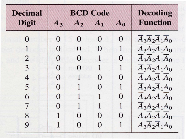
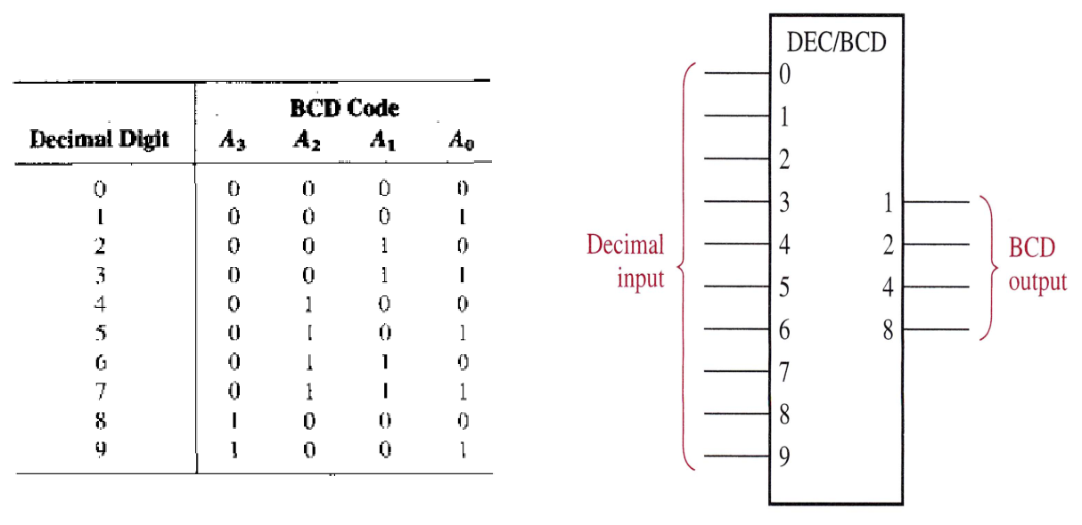
The BCD-to-Decimal Decoder
The BCD-to-Decimal Decoder converts each BCD code (8421 code) into one of ten possible decimal digit indications, usually called 4-line-to-10-line decoder or 1-of-10 decoder.
Truth Table
Logic Symbol & Diagram
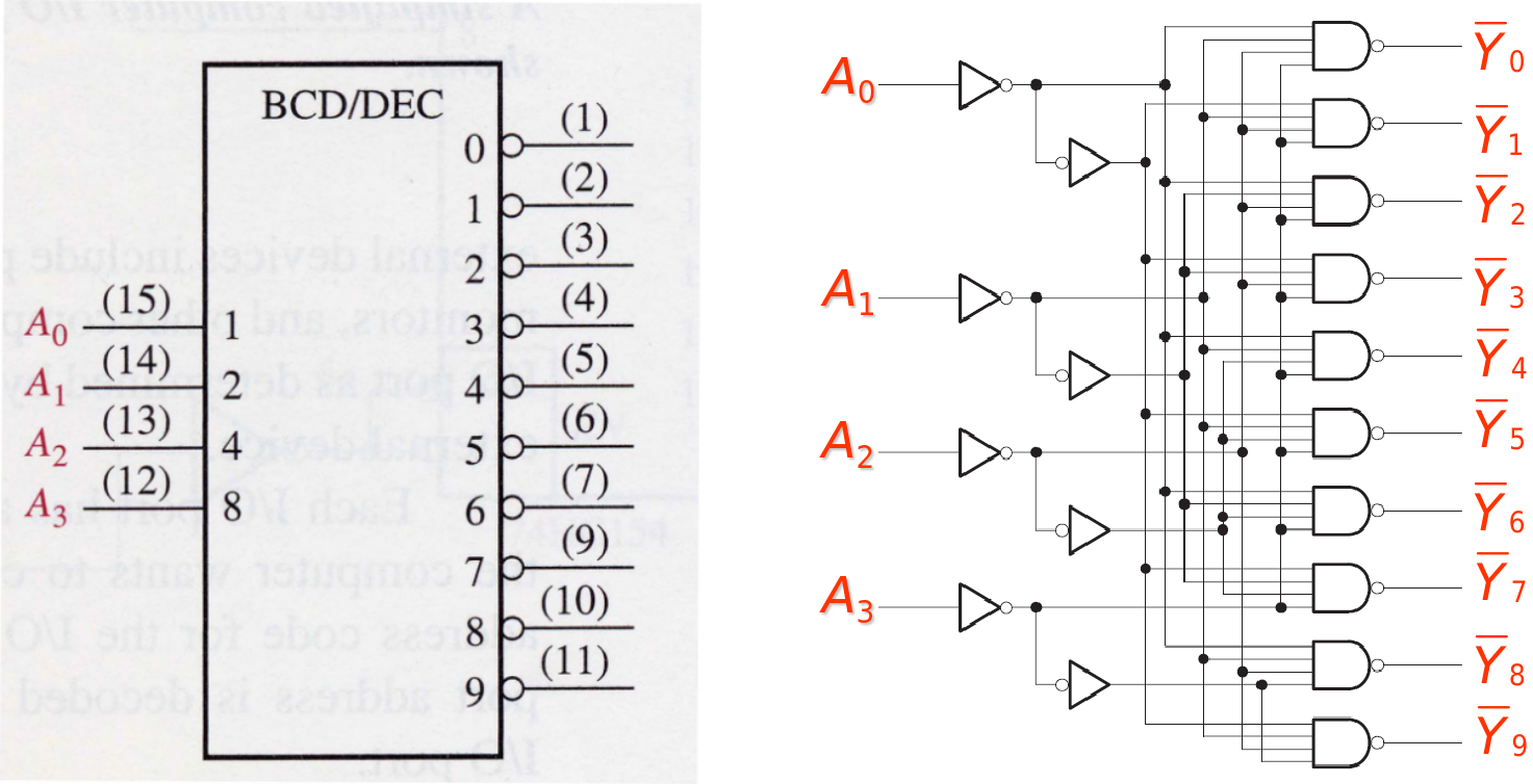
Logic Expression
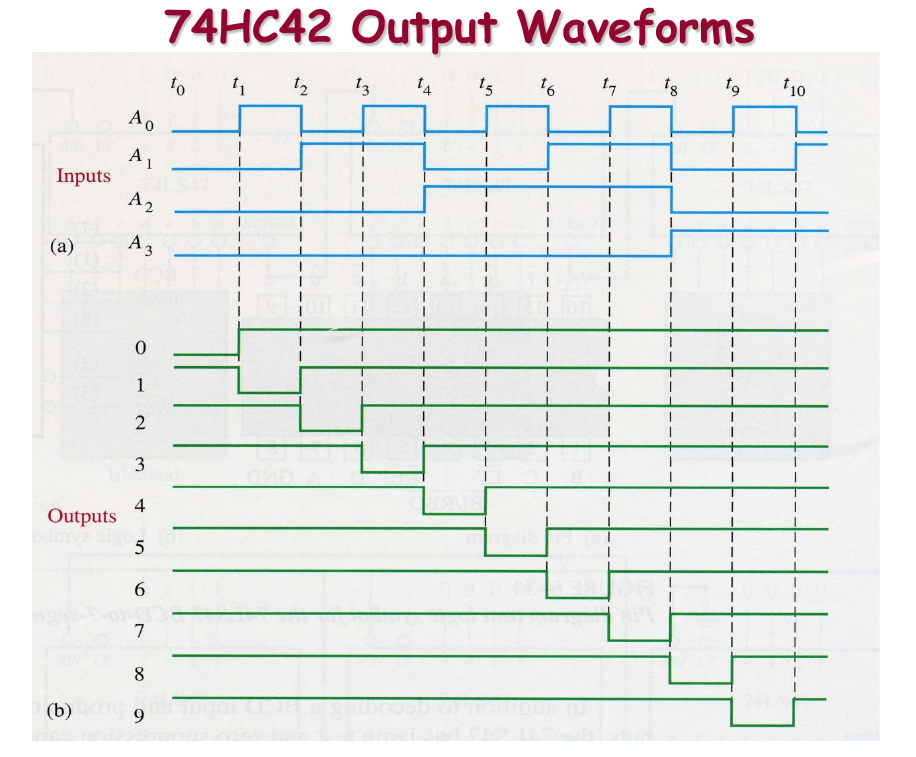
Waveform Example
The BCD-to-7-Segement Decoder
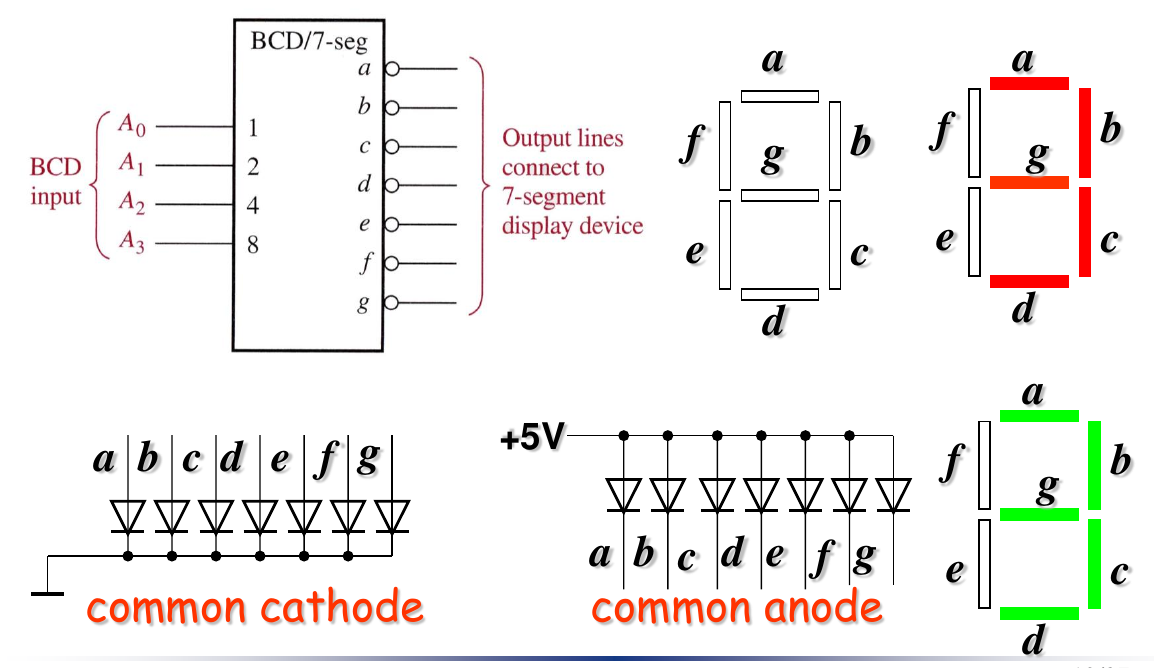
- Common cathode: 共阴极
- 输入高电平的LED段亮,输入低电平的LED段暗
- Common anode: 共阳极
- 输入低电平的LED段亮,输入高电平的LED段暗
Truth Table
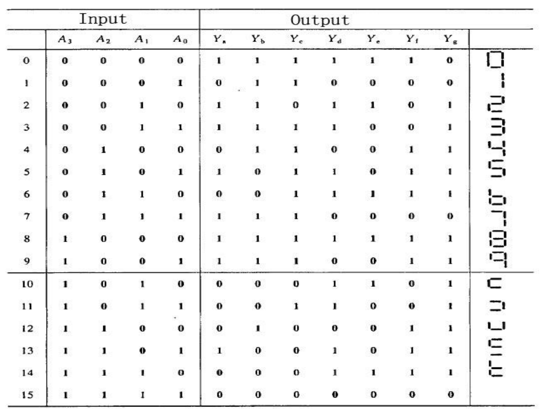
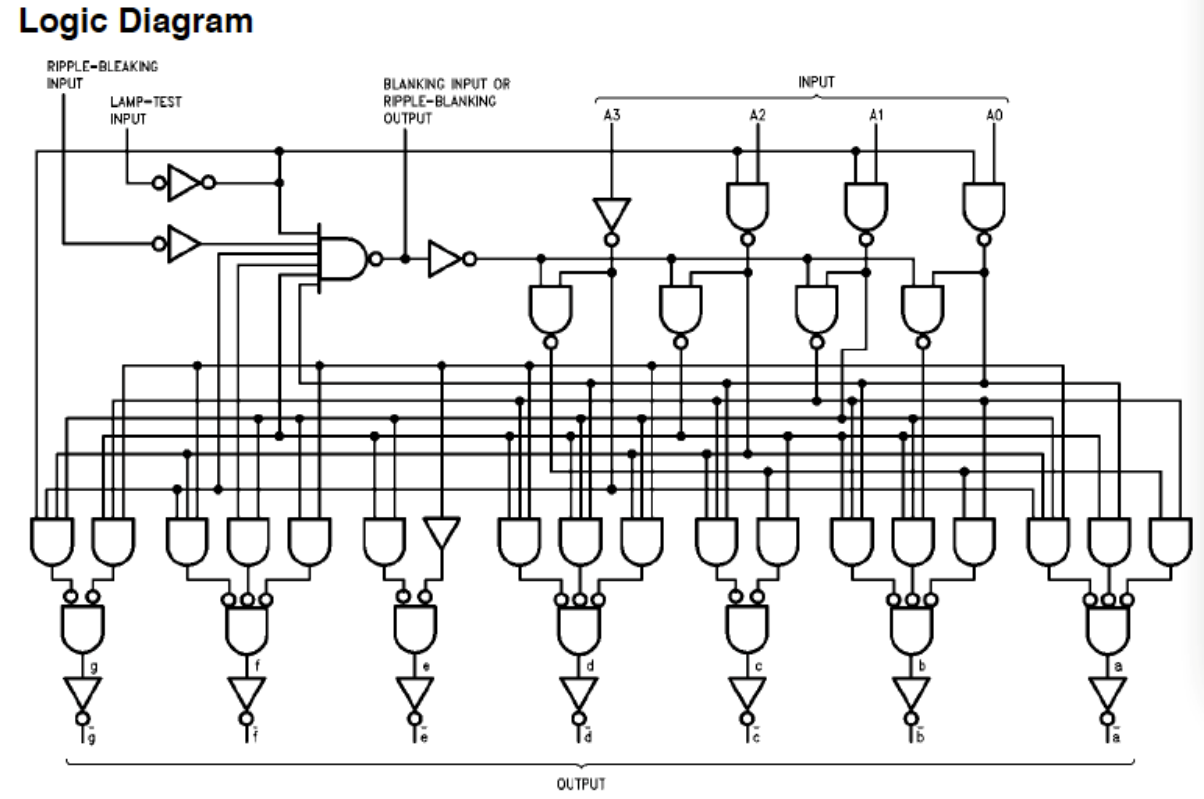
Logic Expression
-
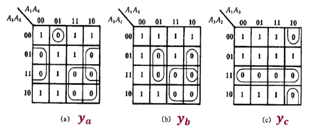
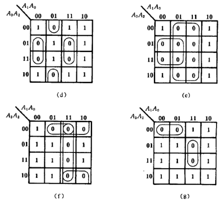
根据真值表,为每一个输出画卡诺图
- 所以写逻辑表达式之前先画真值表
- 每个输出都对应4个输入,所以是4变量卡诺图
-
通过卡诺图最大分组,确定每个输出的最简逻辑表达式
-
写出表达式,自然就知道怎么用逻辑电路实现了
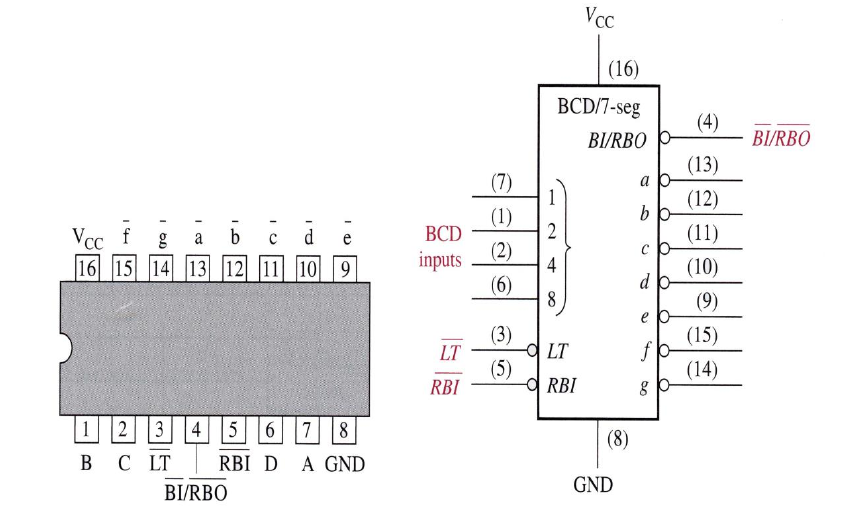
Integrated BCD-7-Segment Decoder
74LS47 is an MSI device that decode a BCD code and drives a 7-segment display.
- The BCD inputs D, C, B, and A are active-HIGH.
- The segment outputs a – g are active-LOW
Input pins definition
- = Lamp Test . When active, all of the 7 segments are turned on. Used to verify no segments are burned out.
- 人话:灯测试,全亮
- = Ripple Blanking Input. When active, all of the 7 segments are turned off if a zero code is on the BCD inputs and RBO will be active.
- 脉冲消隐输入/行波灭零输入
- 工作方式:在一个多位数的显示系统中(比如 4 位显示 “0025”),我们通常不希望显示前面的 “00”。RBI 用于接收来自更高位解码器的“是否需要消隐”的信号。
- 如果 RBI 输入为高电平(通常表示更高位不是零,或者这是最高位且不需要消隐),那么当前这个解码器即使 BCD 输入为 0,也会正常显示 “0”。
- 如果 RBI 输入为低电平(通常表示更高位是零且已经被消隐了),并且当前这个解码器的 BCD 输入也是 0 (0000),那么这个解码器也会被消隐(不显示任何内容),并通过 RBO 输出一个低电平信号给下一位。
- = Blanking Input/ Ripple Blanking Output. When active, all of the 7 segments are turned off.
- 消隐输入 / 脉冲消隐输出
- 作为 BI (Blanking Input - 消隐输入): 当这个管脚被强制设置为低电平(通常情况下)时,它会无条件地关闭所有七段输出(a-g),使得显示器熄灭(Blanking),无论 BCD 输入或 LT 输入状态如何(但有时 LT 会覆盖 BI)。这可以用于完全关闭某个数位的显示。
- 作为 RBO (Ripple Blanking Output - 脉冲消隐输出 / 行波灭零输出): 这个输出状态取决于 RBI 输入和当前的 BCD 输入值。
- 条件: 只有当 RBI 输入为低电平 并且 当前解码器的 BCD 输入为 0 (0000) 时,RBO 输出才会变为低电平。
- 其他情况: 在所有其他情况下(即 RBI 为高电平,或者 BCD 输入不是 0),RBO 输出将保持高电平。
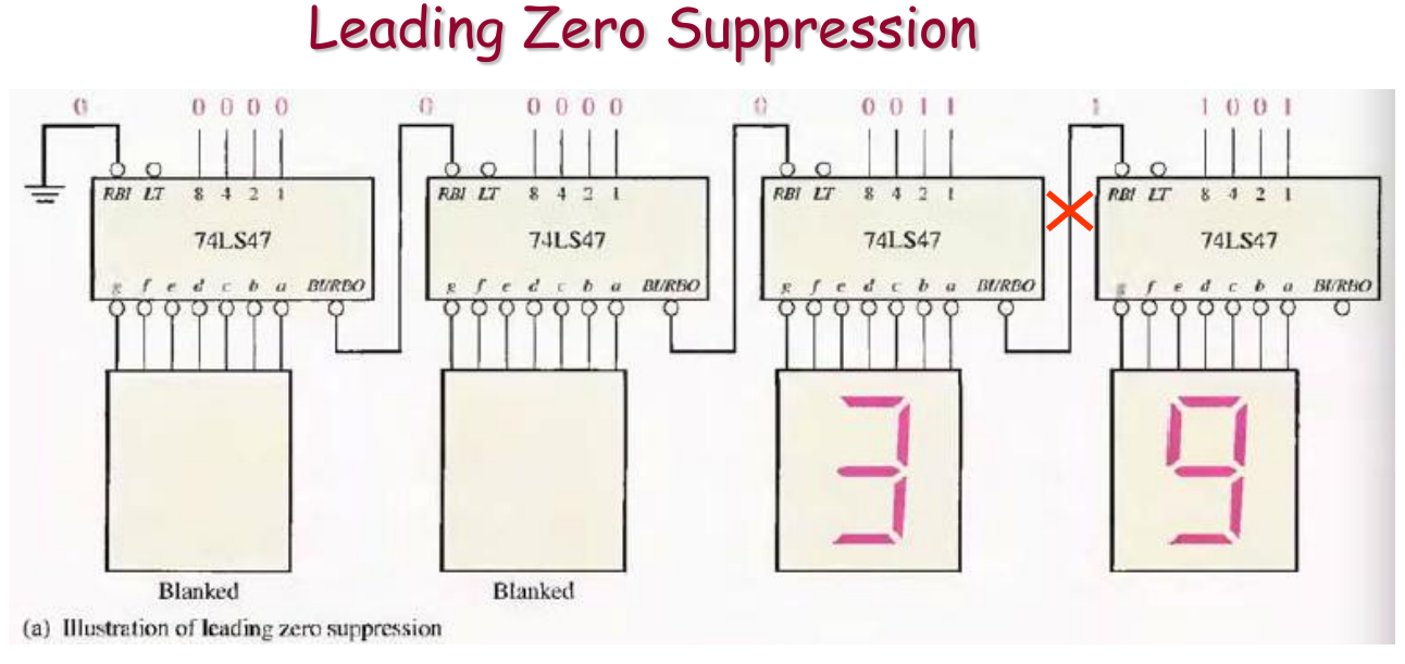
Leading Zero Suppression (前导零抑制)
- 目标: 消除数字整数部分开头多余的零。例如,将 “0075” 显示为 " 75"。
- 方向: 消隐信号从最高位 (MSD) 向最低位 (LSD) 传递。
- 接法:
- 最高位 (MSD) 解码器:
- 将其 RBI (Ripple Blanking Input - 行波消隐输入) 引脚接低电平 (GND)。这使得最高位如果其BCD输入为0,它自身就会被消隐。
- 中间各位解码器:
- 将前一位(更高位)解码器的 RBO (Ripple Blanking Output) 引脚连接到当前位解码器的 RBI 引脚。
- 这个链式连接从MSD的下一位一直持续到LSD的前一位。
- 最低位 (LSD) 解码器:
- 如果希望数字 “0000” 显示为一个 “0”: 将LSD解码器的 RBI 引脚接高电平 (VCC) 或不接。这样即使更高位都因是0而被消隐,LSD也不会被消隐,从而显示出0。
- 如果希望数字 “0000” 完全显示为空白: 则LSD的RBI也按上述链式连接接入(即连接到其前一位的RBO)。
- 最低位(LSD)通常RBO通常不接
- 最高位 (MSD) 解码器:
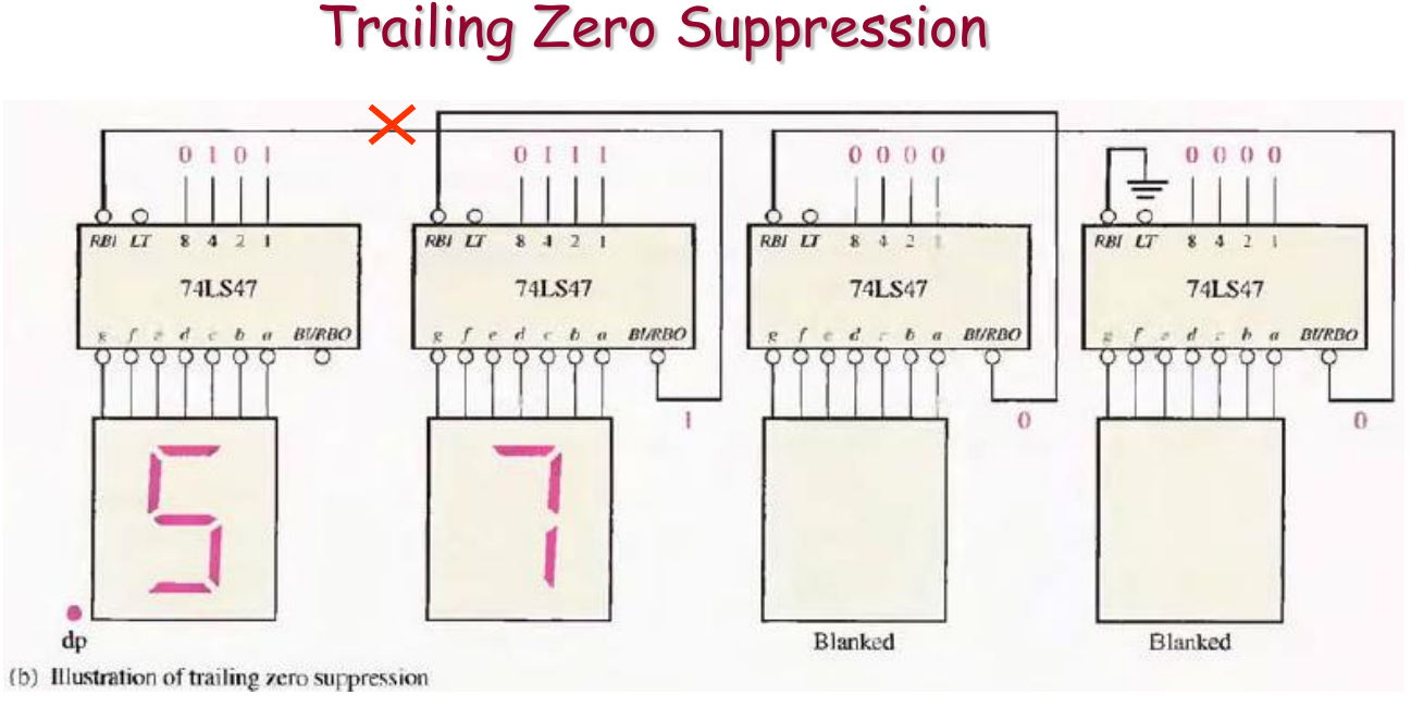
Trailing Zero Suppression (后续零抑制 / 末尾零抑制)
- 目标: 通常用于消除数字小数部分末尾多余的零。例如,将 “12.500” 显示为 “12.5”。
- 方向: 消隐信号从小数部分的最低位 (LSD of fractional part) 向小数部分的最高位 (MSD of fractional part, 即小数点后的第一位) 传递。
- 接法 (仅针对小数部分):
- 小数部分的最低位解码器:
- 将其 RBI 引脚接低电平 (GND)。这使得小数部分的最低位如果其BCD输入为0,它自身就会被消隐。
- 小数部分的中间各位解码器 (从低位向高位):
- 将后一位(更低位)解码器的 RBO 引脚连接到当前位解码器的 RBI 引脚。
- 这个链式连接从小数部分LSD的上一位一直持续到小数点后的第一位。
- 小数点后第一位解码器 (小数部分的最高位):
- 如果希望小数部分
0000显示成一个0,那小数部分的最高位可以接高电平(VCC)或不接 - 如果希望小数部分
0000完全显示成空白,那么其RBI也按上述链式连接接入(即连接到后一位的RBO),就其RBI会接收来自小数部分下一位(更低位)的RBO信号。
- 如果希望小数部分
- 小数部分的最低位解码器:
- 整数部分: 整数部分的解码器通常不参与后续零抑制的RBI/RBO链,它们可能采用前导零抑制的接法,或者不进行任何消隐。
实际用的时候不太用这些原始方法做零抑制的,用MCU编写程序处理零抑制和小数点位置,更灵活和方便。
6.4 Encoders
- An encoder is a combinational logic circuit that essentially performs a “reverse” decoder function.
- An encoder accepts an active level on one of its inputs representing a digit, such as a decimal or octal digit, and converts it to a coded output, such as BCD or binary. Encoders can also be devised to encode various symbols and alphabetic characters. The process of converting from familiar symbols or number to a coded format is called encoding.
The Decimal-to-BCD Encoder
The decimal-to-BCD encoder has ten inputs – one for each decimal digit and four outputs corresponding to the BCD code.
Simple Encoder
This kind of encoder works only when one input is active (HIGH) at a time, otherwise it will result in incorrect outputs.
Priority Encoder
The priority function means that the encoder will produce a BCD output corresponding to the highest-order digit input that is active and ignore any other lower-order active inputs.
8-Line-to-3-line priority encoder
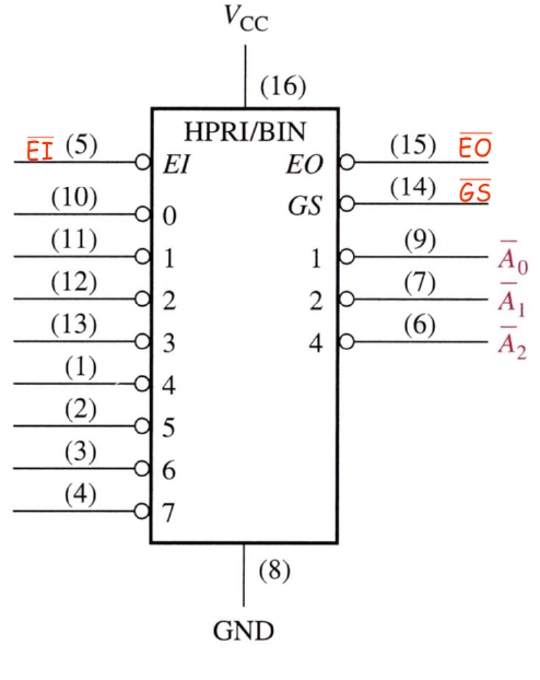
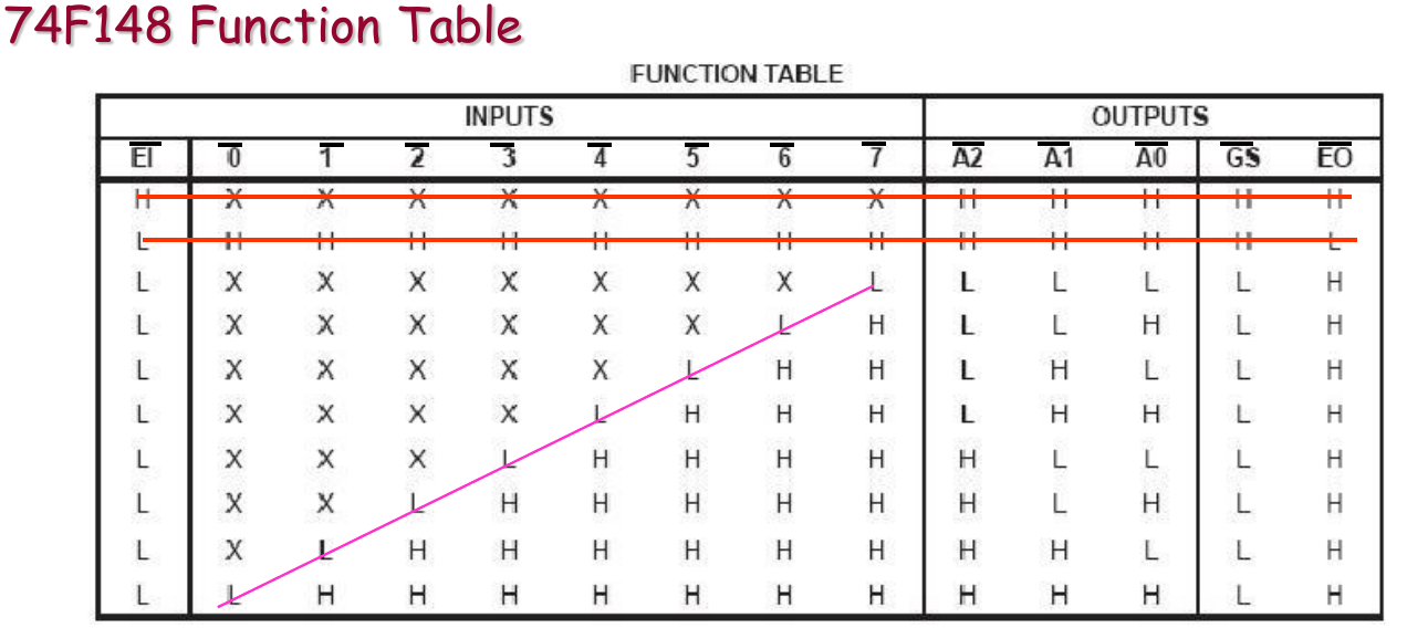
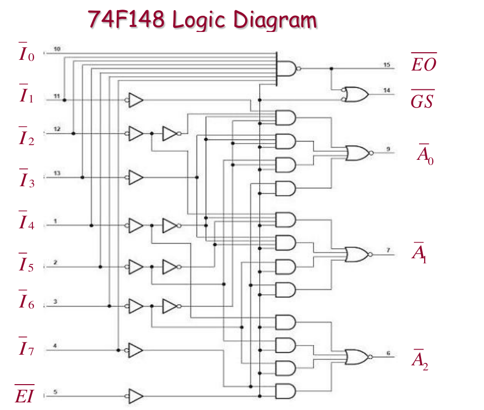
74F148 is a 8-Line-to-3-line priority encoder that has eight active-LOW inputs and three active-LOW binary outputs. The device can be used for converting octal inputs to a 3-bit binary code.
- All inputs and outputs are active LOW.
- = Enable Input. When inactive, all outputs are deactivated.
- = Enable output. EO is active if EI is active and none of the inputs is active.
- = Gate Strobe. GS is active if EI is active and any of the inputs is active.
Truth Table
Logic Expression
Logic Diagram
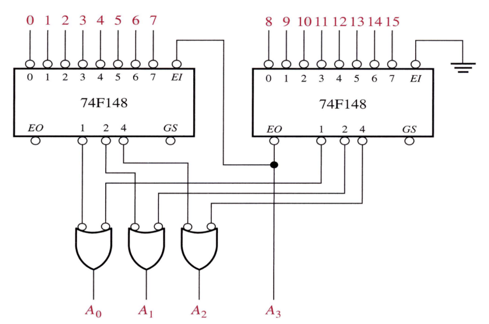
Expansion: 16-4 Priority Encoder
The Decimal-to-BCD Priority Encoder
The Decimal-to-BCD priority encoder means that the encoder will produce a BCD output corresponding to the highest-order decimal digit input that is active and ignore any other lower-order active inputs.
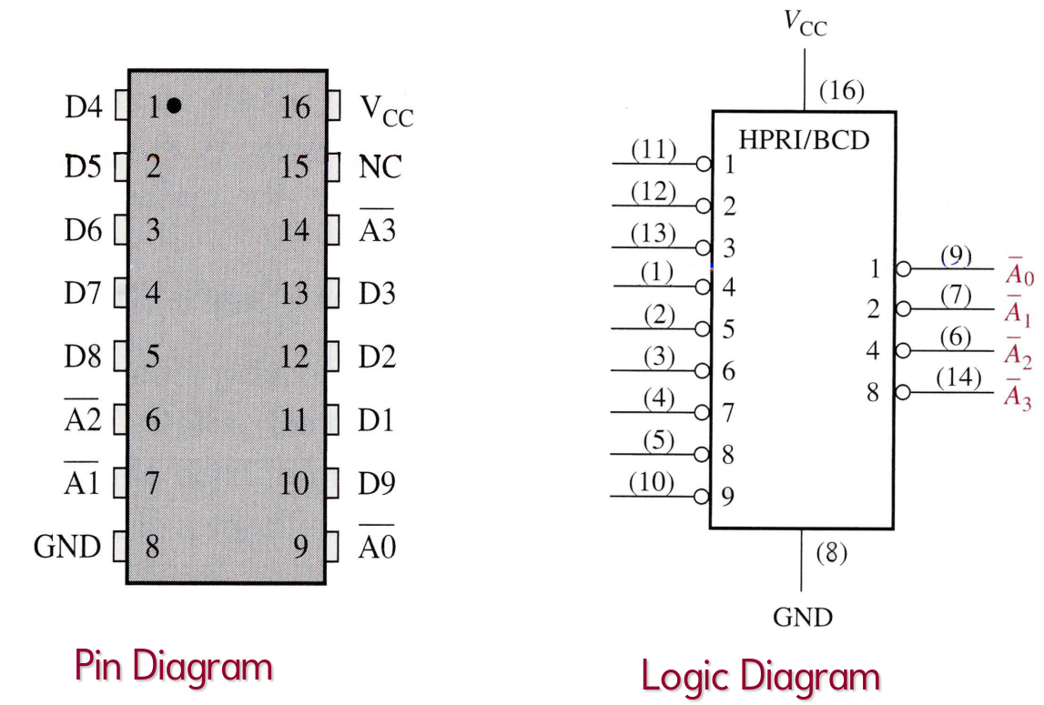
- 74HC147 is a priority encoder with active-LOW inputs (0) for decimal digits 1 through 9, and active-LOW BCD outputs. A BCD zero output is represented when none of the inputs is active.
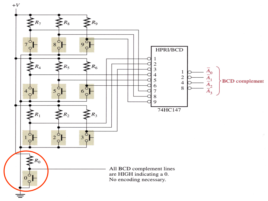
Application example: Simplified keyboard encoder
6.5 Code Converters
A code converter converts one code to another.
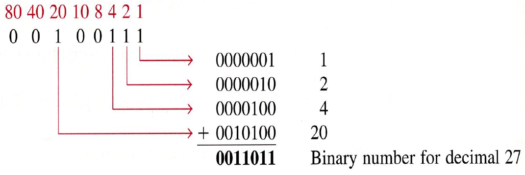
BCD-Binary Conversion
- Determine the value or weight of each bit in the BCD number, and represent it by a binary number;
- Add all the weights that the corresponding bits are 1s;
- The result of this addition is the binary equivalent of the BCD number.
Example
Convert the BCD numbers 0010 0111 to binary
- The weights of each bit as follows:
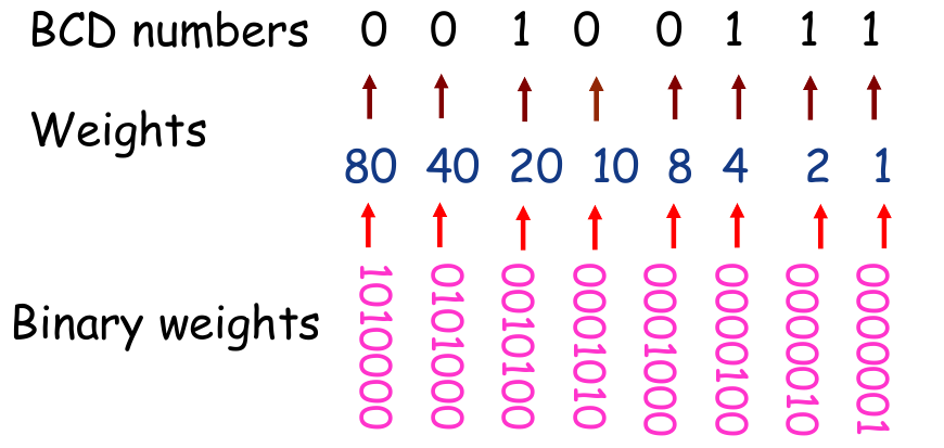
- Sum of the weights:
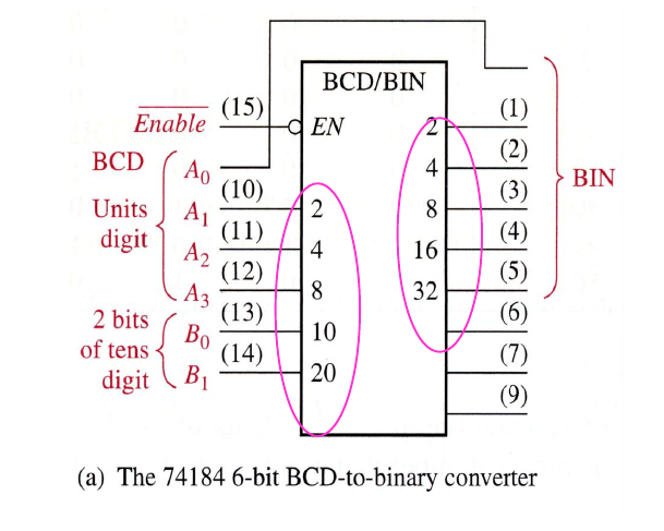
Integrated Conversion Chip
一个有趣的现象: 不需要处理,因为BCD码的LSB和对应二进制的LSB必然是一致的(想一想就能明白)
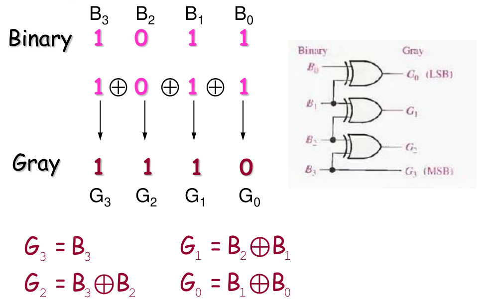
Binary-to-Gray Conversion
- XOR gates can be used for the conversions
- 记住:如果要画二进制/格雷码互转的逻辑电路图,从MSB开始画
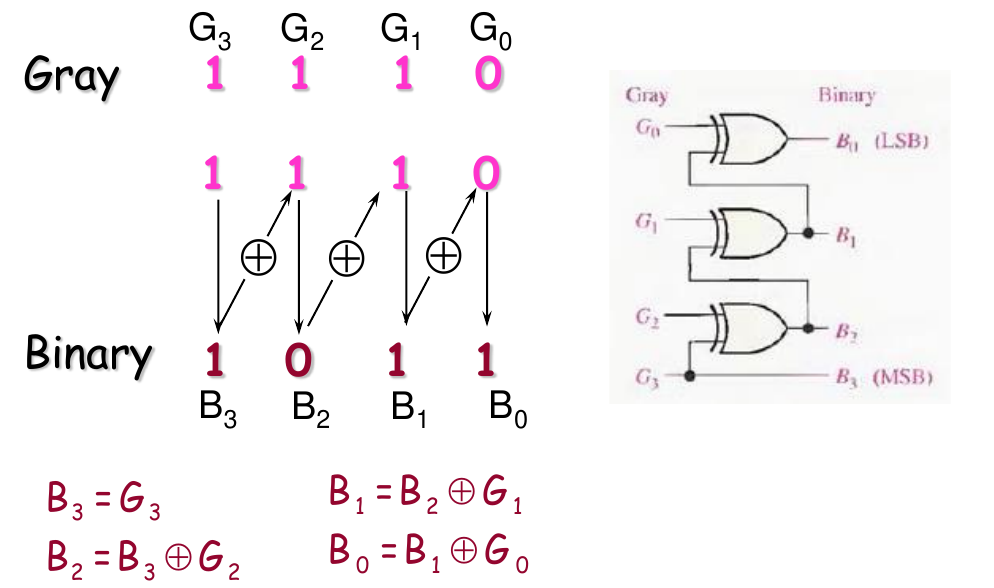
Gray-to-Binary Conversion
- XOR gates can be used for the conversions
- 记住:如果要画二进制/格雷码互转的逻辑电路图,从MSB开始画
- 注意:处理一位Gray Code的XOR Gate的输入连的是这一位的Gray Code和高一位的Binary Code转换结果,MSB直接输出,与Binary转Gray是不同的,别搞混了
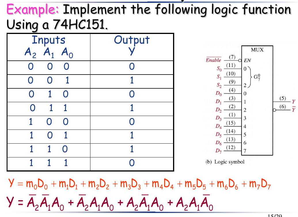
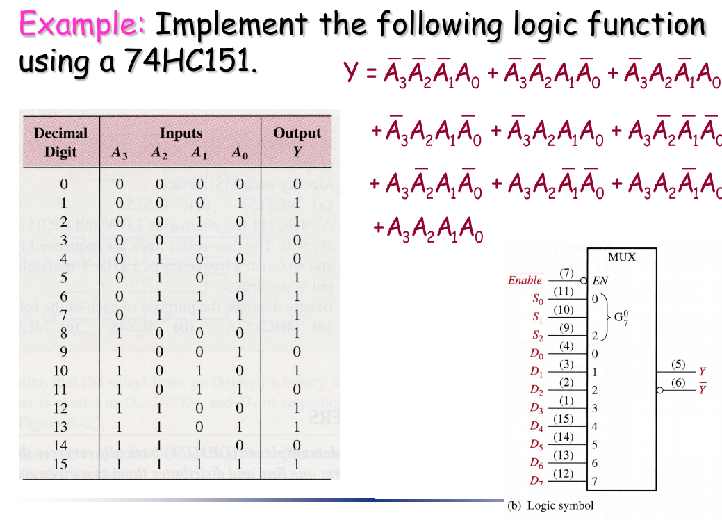
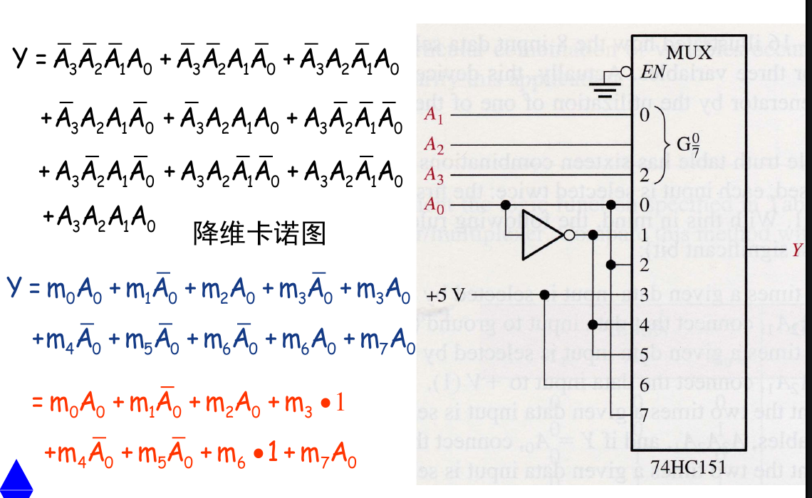
6.6 Multiplexers
A multiplexer (MUX) is a device that allows digital information from several sources to be routed onto a single line for transmission over that line to a common destination.
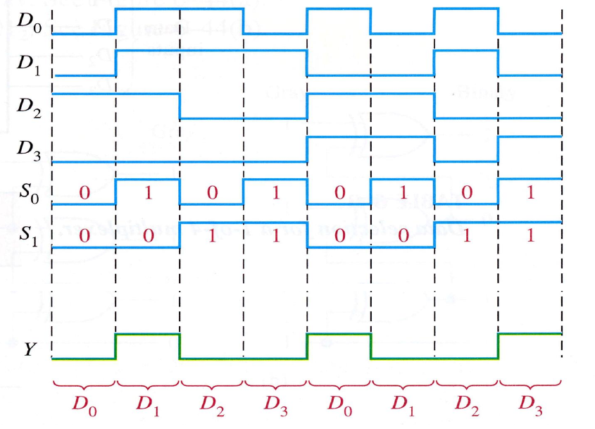
4-bit data selector
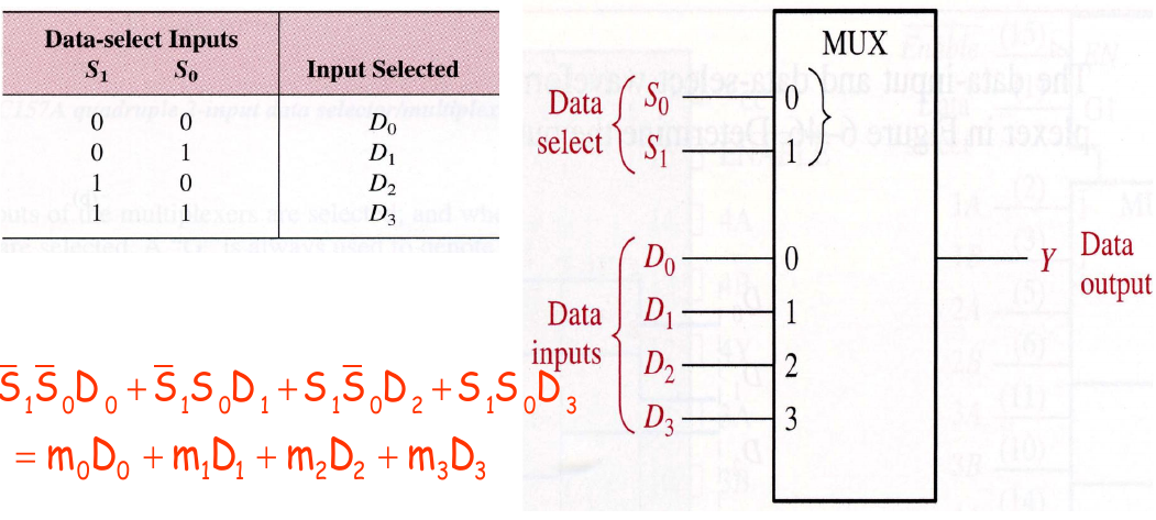
Logic Expression
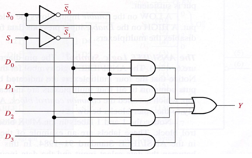
Logic Diagram
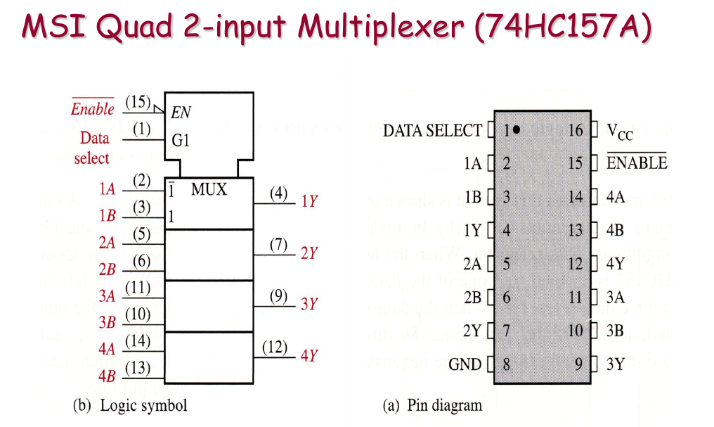
Integrated Multiplexer
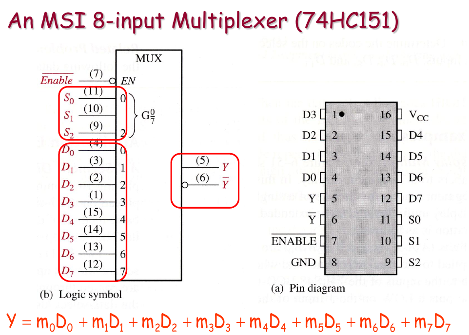
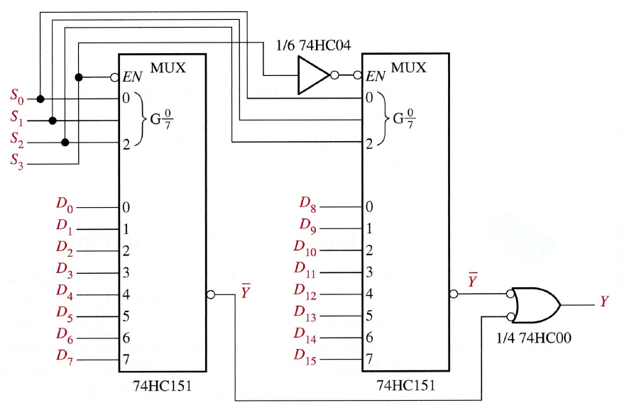
Expansion
例题
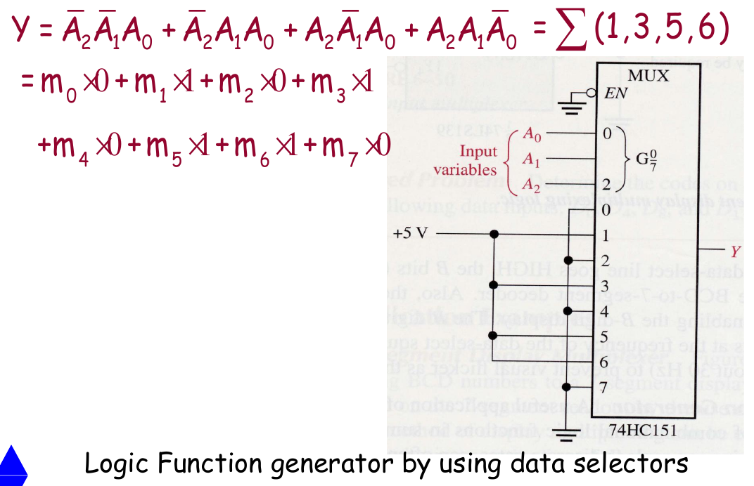
- 一个技巧:“降维卡诺图“。具体来说就是把三个变量作为选通用的变量(作为卡诺图的变量),剩下的一个变量作为数据输入当作常数写进卡诺图的单元格中,专门用来解下面这种题
6.7 Demultiplexers
A demultiplexer (DEMUX) basically reserves the multiplexing function. It takes data from one line and distribute them to a given number of output lines. For this reason, the demultiplexer is also known as a data distributor.
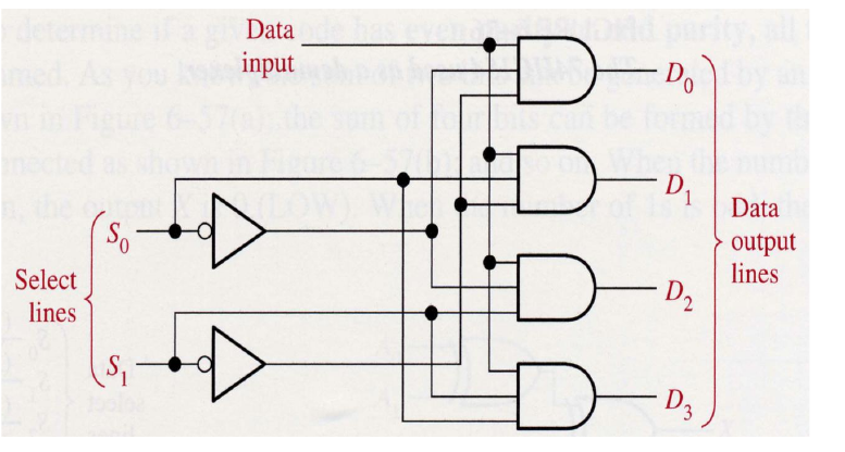
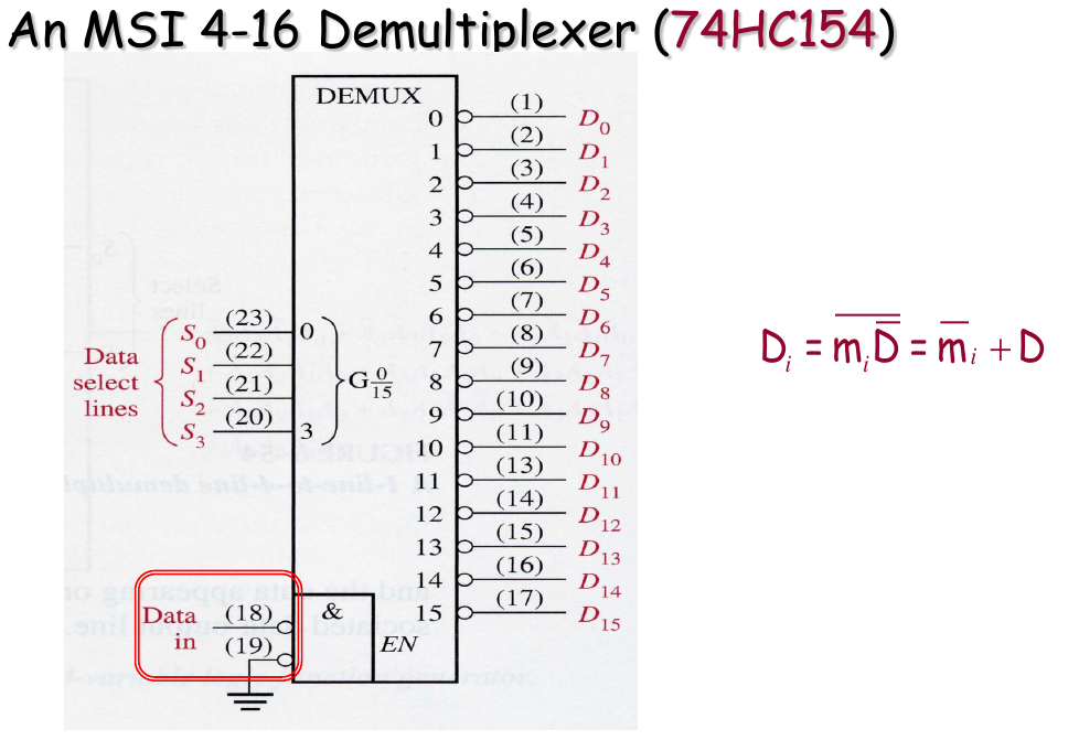
Logic Expression
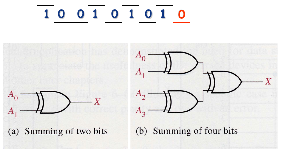
6.8 Parity Generators/Checkers
- Parity method uses a parity bit as a means for bit error detection.
- A parity bit is attached to a group of bits to make the total number of 1s in a group always even or always odd.
- Basic Parity Logic:
- The sum of an even number of 1s is always 0
- the sum of odd number of 1s is always 1
Basic Structure
- Summing by XOR Gates
Integrated Parity Generator/Checker
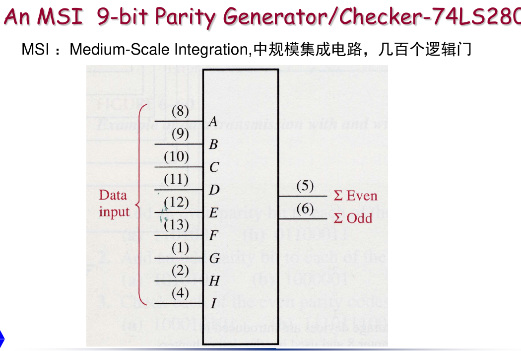
Parity Checker: When the device is used as an even parity checker, the number of input bits that are highs should always be Even; and when a parity error occurs, the Even output goes LOW and the Odd goes HIGH.
Parity Generator:
- For even parity generator, take Odd output as the parity bit;
- For odd parity generator, take Even output as the parity bit.