Chapter7 Latchs, Flip-Flops and Timers
- Latchs 锁存器
- Flip-Flops 触发器
- Timers 计时器
- Bistable(双稳态) devices have two stable states, called SET and RESET. They are used as storage devices.
- Monostable(单稳态) devices (monostable trigger, one-shot) have one stable state. They are used as timers.
- Astable devices (multivibrator) (多谐振荡器) do not have stable state. They are used as waveform generators(波形发生器).
7.1 Lateches
- The latch is a type of temporary device that hastwo stable states (bistable) for storing a bit and is normally placed in a category separate from that of flip-flops.
- The difference between latches and flip-flops isthe method used for changing their states.
- 简要理解,跟着时钟改变状态的是flip-flop,不跟着时钟改变状态的是锁存器
S-R Latch
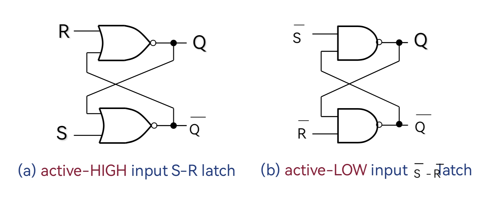
active-HIGH S-R Latch
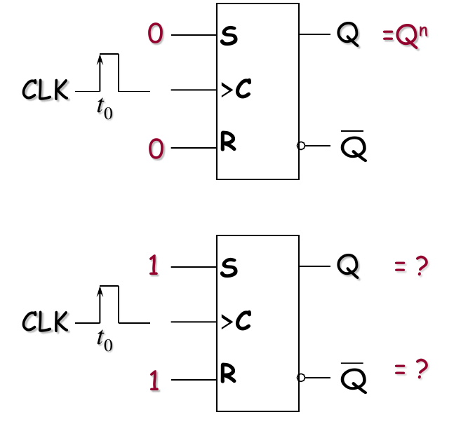
- 只要S和R都设置为0,则触发器处于稳态,保持当前状态不变
- S=1 R=0 则触发器置位,输出变为
- S=0 R=1 则触发器复位,输出变为
- S=1 R=1 无效状态,输出为
Truth Table
| S | R | (当前状态) | (下一状态) | 说明 |
|---|---|---|---|---|
| 0 | 0 | 0 | 0 | 保持 (No Change) |
| 0 | 0 | 1 | 1 | 保持 (No Change) |
| 0 | 1 | 0 | 0 | 复位 (Reset) |
| 0 | 1 | 1 | 0 | 复位 (Reset) |
| 1 | 0 | 0 | 1 | 置位 (Set) |
| 1 | 0 | 1 | 1 | 置位 (Set) |
| 1 | 1 | 0 | 0* | 不允许 (Invalid) |
| 1 | 1 | 1 | 0* | 不允许 (Invalid) |
逻辑表达式
在假设 (即 S 和 R 不会同时为 1) ,即认为S 和 R 同时为高电平表示为 X (Don’t Care)的条件下,可以得出简化版逻辑
The Gated S-R Latch
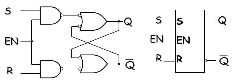
直接给结论:
- 时,S(置位)和R(复位)才会起作用
- 时,无论S和R的值如何,Q和的输出均表示不变
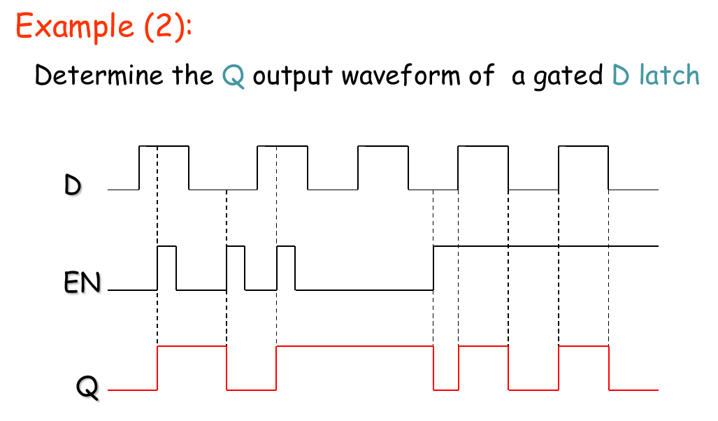
The Gated D Latch
当时,
- 时,Q的值随D改变
- 时,Q的值被锁存,无论D怎么变,Q和的值均不变
完整的逻辑表达式
7.2 Edge-Triggered Flip-Flops
- Flip-flops are synchronous bi-stable devices.
- The term synchronous means that the output changes state only at a specified point on a triggering input called the clock (CLK) which is designated as a control input C; that is, changes in the output occur in synchronization with the clock.
- An edge-triggered flip-flop changes state either at the positive edge (rising edge) or at the negative edge (falling edge) of the clock pulse and is sensitive to its input only at this transition of the clock.
Edge-Triggered S-R Flip-Flops

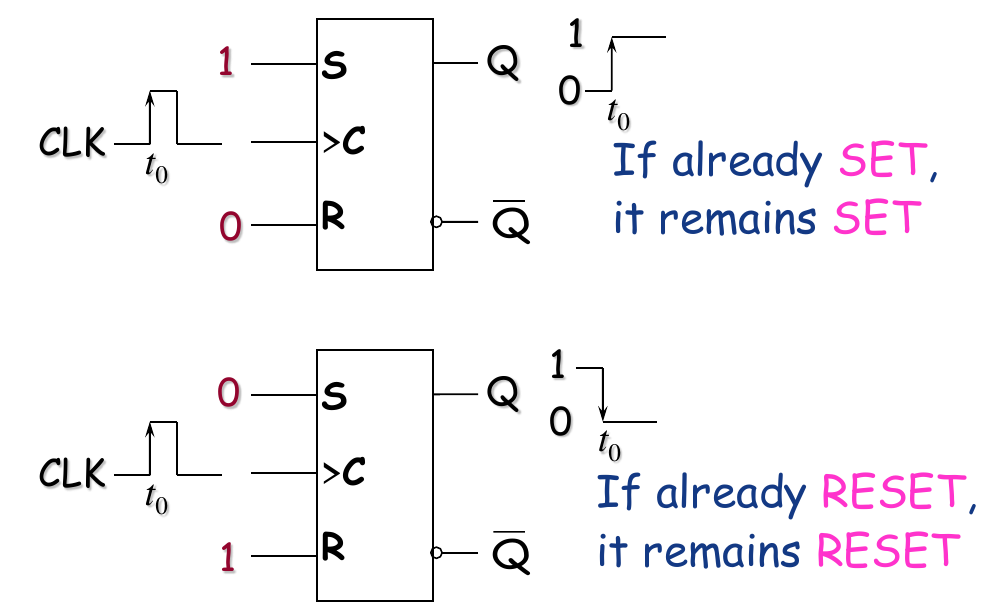
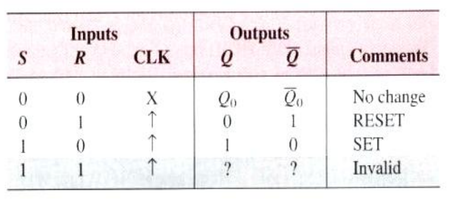
- When S is HIGH and R is LOW on the triggering edge of the clock pulse, Q is HIGH and the flip-flop is SET.
- When S is LOW, R is HIGH, Q is LOW and flip-flop is RESET.
- When S and R are both LOW, the output does not change from its prior state.
- When S and R are both HIGH, it is an invalid condition.
Truth Table
 $$
\begin{cases}
Q^{n+1} = S + \overline{R} Q^{n} \\
S \cdot R = 0
\end{cases}
$$
$$
\begin{cases}
Q^{n+1} = S + \overline{R} Q^{n} \\
S \cdot R = 0
\end{cases}
$$
- Only change at the triggering edge (often rising edge) of CLK (clock pulse)
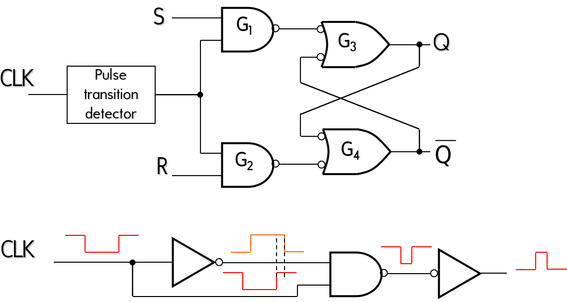
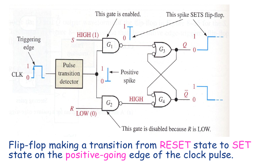
A Method of Edge-Triggering
- 非常巧妙,利用非门的延迟在时钟上升沿创造一个短暂的高电平,从而Enable Gate

The Edge-Triggered D Flip-Flop
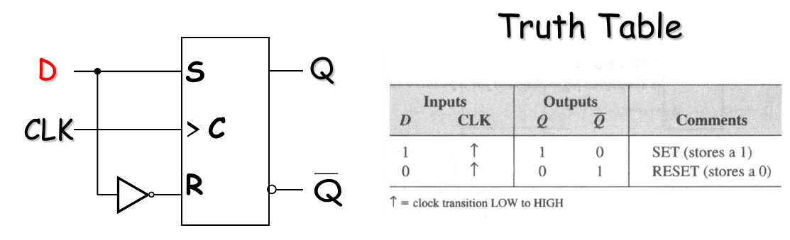 $$
Q^{n+1} = D
$$
$$
Q^{n+1} = D
$$
- Only change at the triggering edge of CLK (clock pulse)
The Edge-Triggered J-K Flip-Flop

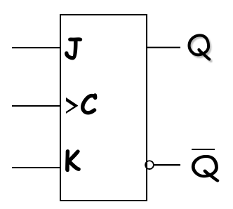
Truth Table
| J | K | CLK | Q | 注释 (Comments) | |
|---|---|---|---|---|---|
| 0 | 0 | ↑ | 保持 (No change) | ||
| 0 | 1 | ↑ | 0 | 1 | 复位 (RESET) |
| 1 | 0 | ↑ | 1 | 0 | 置位 (SET) |
| 1 | 1 | ↑ | 翻转 (Toggle) |
Logic Expression
Asynchronous Preset and Clear Inputs
-
异步性 (Asynchronous):
- 这两个输入之所以被称为“异步”,是因为它们不需要等待时钟脉冲 (CLK) 的有效边沿即可对触发器的输出状态产生影响。
- 它们可以立即改变触发器的状态,优先于同步输入(如 J、K、D、T)和时钟信号。
-
预置 (Preset, PRE):
- 预置输入通常用于将触发器的输出 Q 强制设置为逻辑 ‘1’ (高电平),同时其反向输出 被强制为逻辑 ‘0’。
- 这个操作也常被称为“置位 (Set)”。
-
清除 (Clear, CLR):
- 清除输入通常用于将触发器的输出 Q 强制设置为逻辑 ‘0’ (低电平),同时其反向输出 被强制为逻辑 ‘1’。
- 这个操作也常被称为“复位 (Reset)”。
-
优先级 (Priority):
- 异步输入通常具有最高优先级。也就是说,如果一个有效的异步输入信号出现,它将覆盖所有其他同步输入和时钟信号的作用。
- 在实际应用中,需要注意当 和 同时处于有效状态(例如,都为低电平)时的情况。这种状态通常是不允许的或会导致不确定的输出,具体行为取决于触发器的内部设计。
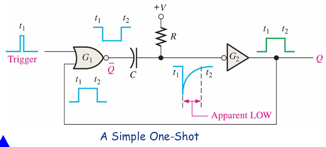
One-Shots
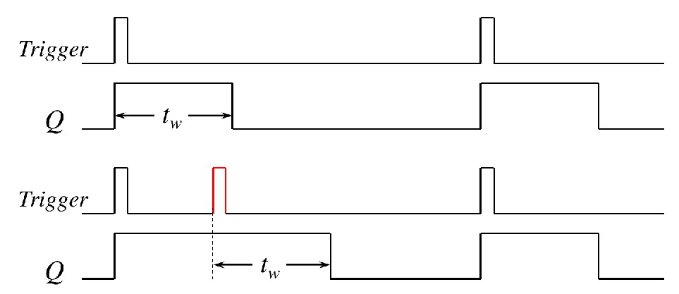
The one-shot is a monostable device, that is, it has only one stable state. A one-shot is normally in its stable state and will change to its unstable state only when triggered. Once it is triggered, the one-shot remains in its unstable state for a predetermined length of time and then automatically returns to its stable state. The time that the device stays in its unstable state determines the pulse width of its output.
- A single narrow trigger pulse produces a single output pulse whose time duration is controlled by the RC time constant.
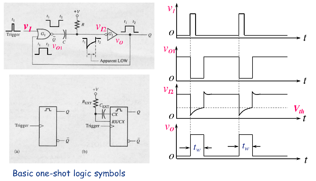
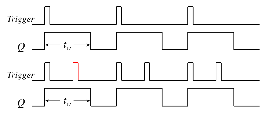
Nonretriggerable One-Shot
A nonretriggerable one-shot will not respond to any additional trigger pulses from the time it is triggered into its unstable state (fired) until it returns to its stable state.
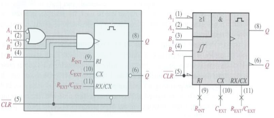
MSI: Nonretriggerable One-Shot 74121
- The inputs A₁, A₂, and B are trigger inputs.
- The terminal connects to a internal timing resistor.
- The and / terminals connect external timing capacitor and resistor.
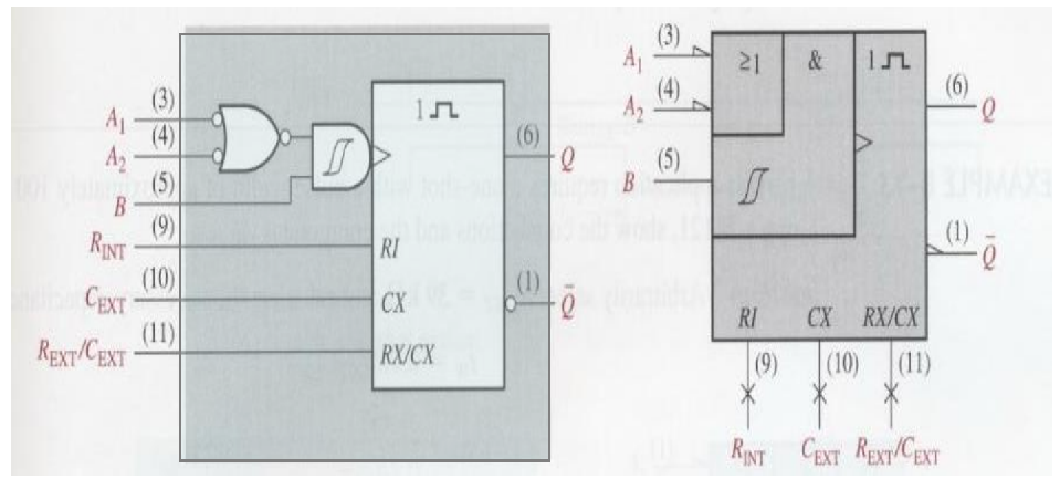
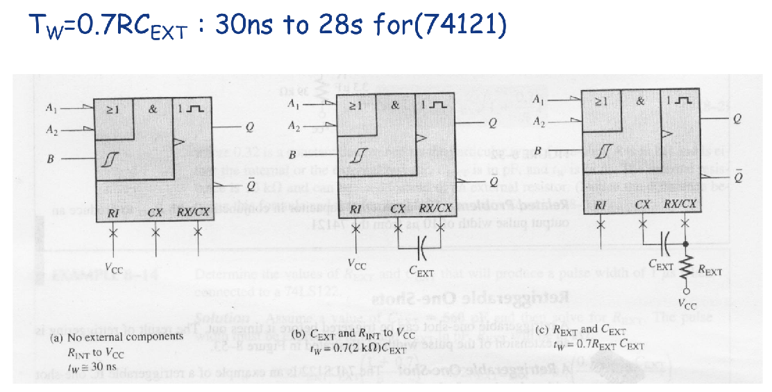
With no external resistor and capacitor:
With external resistor and capacitor:
- internal resistor
Retriggerable One-Shots
A retriggerable one-shot can be triggered before it times out.
MSI: retriggerable One-Shot 74LS122
- With no external resistor and capacitor:
- With external resistor and capacitor:
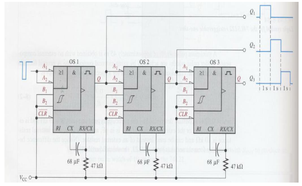
Sequential Pulse Generator
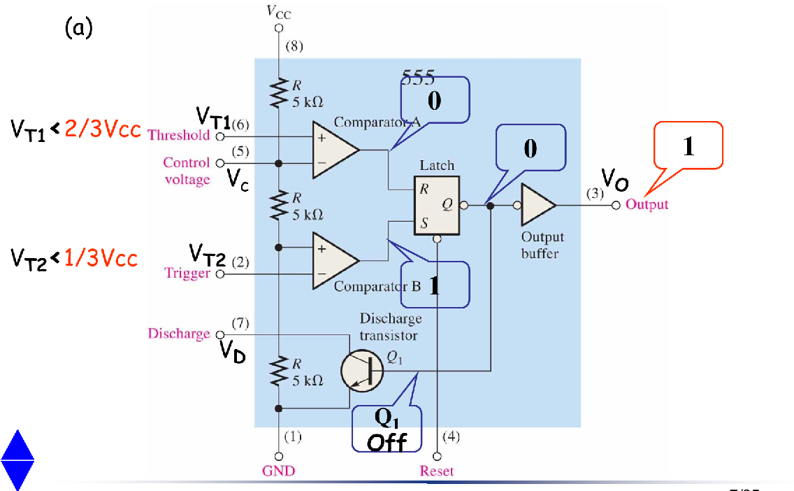
The 555 Timer
The 555 timer is a versatile and widely used device because it can be configured in three different modes as either a Schmitt trigger, a monostable multivibrator (one-shot), or an astable multivibrator (oscillator).
- 三种主要工作模式
- 非稳态多谐振荡器 (Astable Multivibrator) - 振荡器模式
- 单稳态多谐振荡器 (Monostable Multivibrator) - 单次触发模式
- 双稳态多谐振荡器 (Bistable Multivibrator) 或 施密特触发器 (Schmitt Trigger) 模式
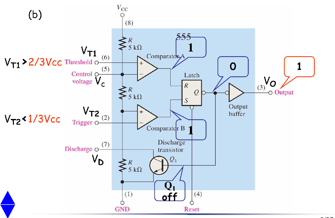
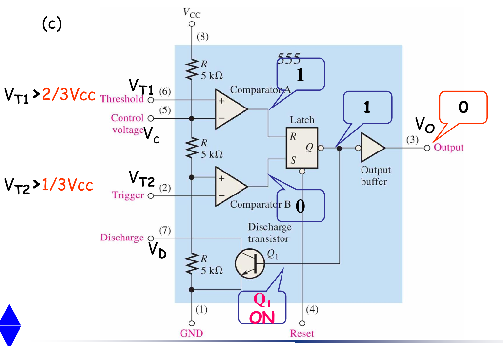
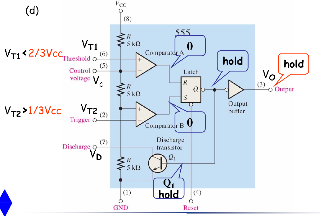
四种基本状态
- 这四种状态就对应里面那个S-R Latch的四种状态
- SET
- RESET
- HOLD
- INVALID
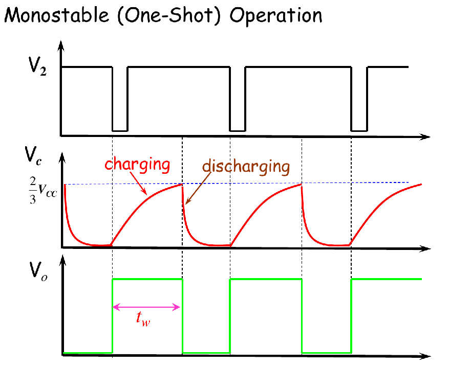
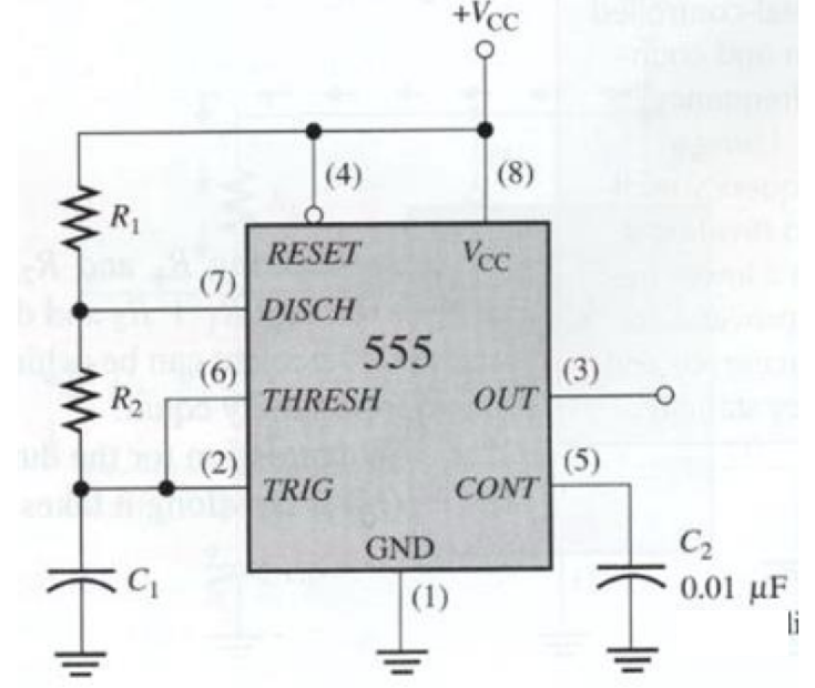
Monostable (One-Shot) Operation 单稳态触发器
- 电路连接特征
- (2) trigger 作为触发器输入,低电平有效(下降沿触发)
- (6) Threshold 接RC中间 GND-C-(6)-R-VCC
- (7) Discharge 也接RC中间
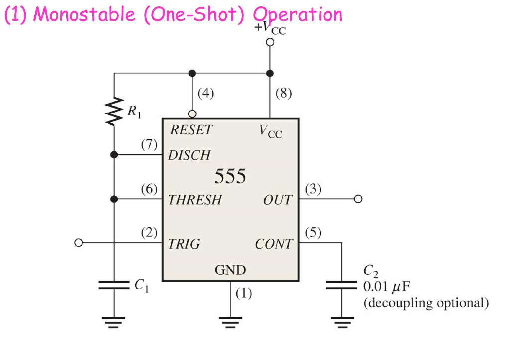
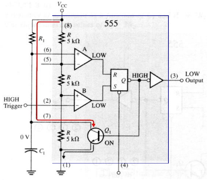
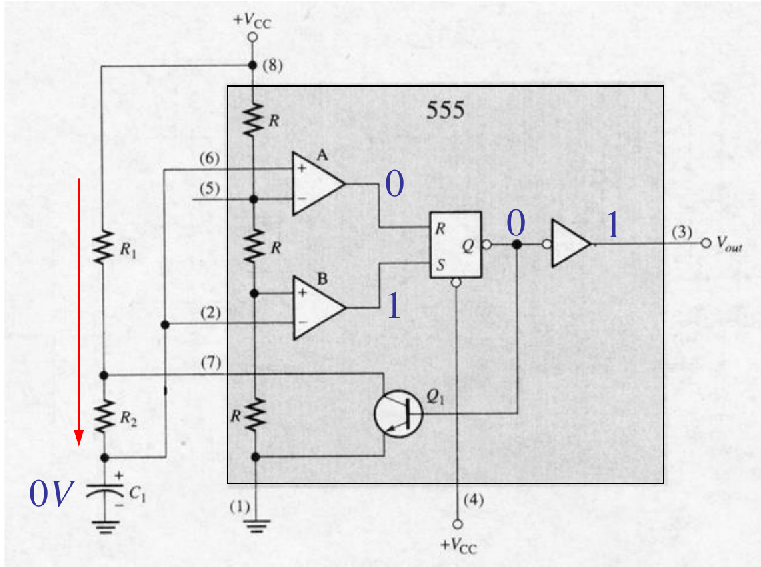
Initial State (Prior to Triggering) 初始状态
Assume the initial state is
- S-R Latch is in RESET state, and is holding (R/S pins are all LOW)
- Trigger pin is HIGH
- Discharge BJT is in the ON state
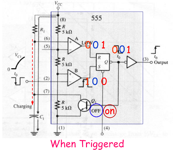
When Triggered
- A LOW (A Falling Edge) appears at Trigger pin
This will cause
- S-R Latch is SET, Q becomes HIGH, becomes LOW
- is off, RC Circuit starts charging,
Return to Initial State
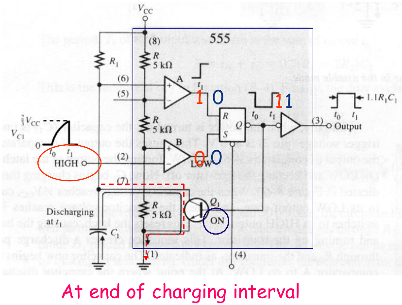
When reaches , the S-R Latch is RESET, and then
- is on, the capacitor quickly discharges through
- becomes low again, the S-R Latch holds at RESET state.
- Remember the Conclusion
Invalid State
- If the LOW continues appearing at Trigger after, the S-R latch will stay enter invalid state, which in most S-R Latch setups, the output Q is still SET.
- Q will remain HIGH
- 一直持续输出高电平
- 电容持续充电直到
- 一般来说,不要出现这种情况
Default is non-retriggerable
- 默认不可重复触发
- 若需重复,需要添加一个比较复杂的外置电路(应该不会考)
Astable Operation
电路连接
When the power is turned on
- begins charging
C1 Repeatedly switch between charging and discharging
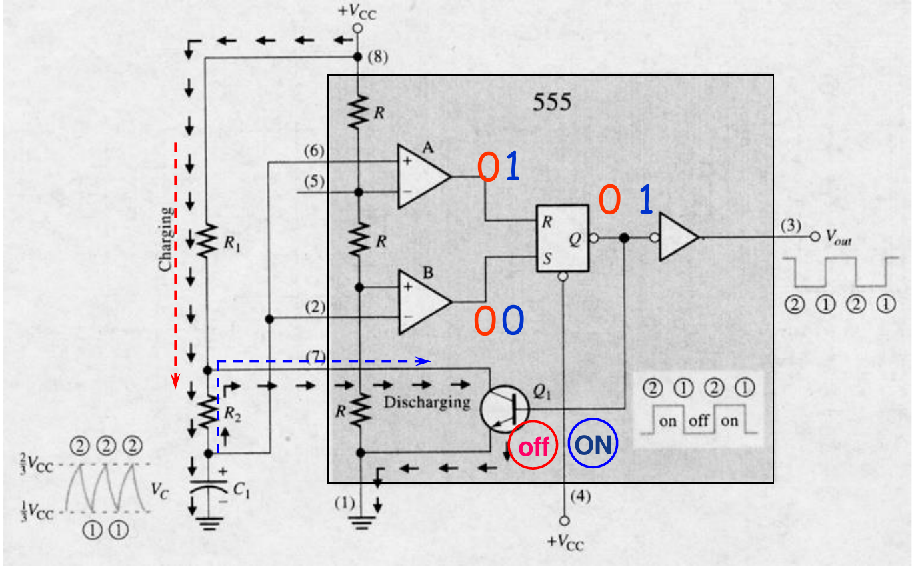
- 充到 时, S-R Latch复位,Q变LOW,放电三极管打开,C1开始放电
- 放到 时,S-R Latch复位,Q变LOW,放电三极管关闭,C1开始充电
- 充电时 输出高电平, 放电时 输出低电平
- 放电电路由和构成,充电电路由和构成,所以充/放电的时间常数就很显而易见
- 最终结果: 周期性地在充电/放电之间切换, 产生方波输出
Any Duty Cycle
施密特触发器模式 Schimitt Trigger/Bistable operation
A Simple Schmitt Triggerc
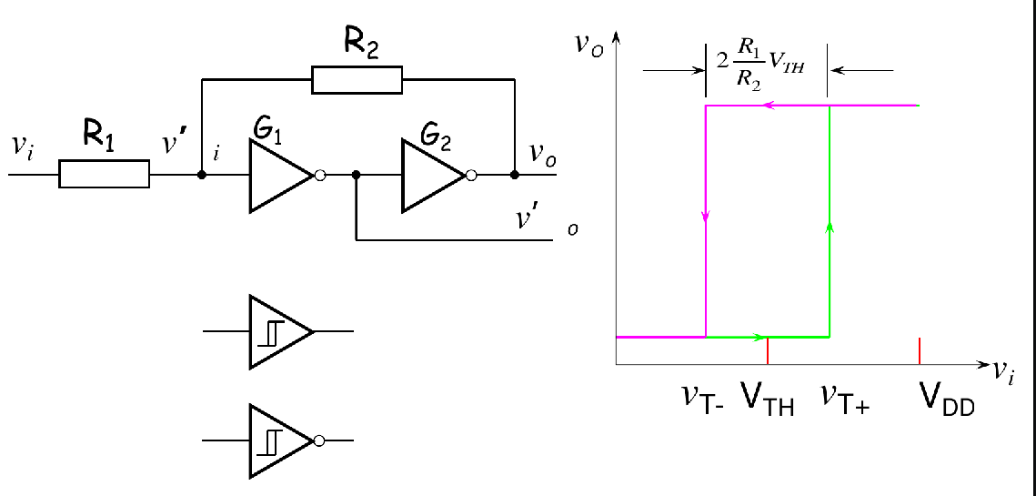
迟滞宽度为
假设理想状况高低电平的界限(阈值电压)是
的话,那么有结论:迟滞宽度为
555 Timer Schimitt Trigger Operation
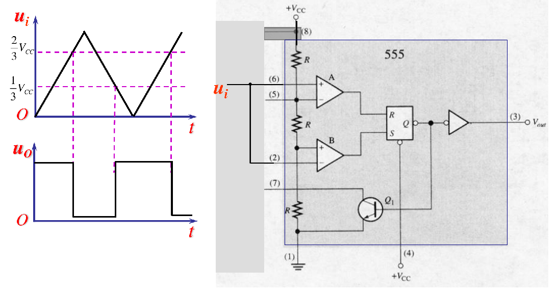
- 该模式下的电路连接
- (2) trigger和(6) threshold接一起,作为电压输入
- 还记得滞回比较器么,这个分析方法差不太多很简单
- 默认初始状态S-R Latch为RESET状态,初始电压的情况下,逐渐增加到超过上升阈值,然后再减小到小于,回到RESET状态,就能把整个滞回曲线画出来了
- 结论: