Chapter8 Counters
- Flip-flops can be connected together to perform counting operations. Such a group of flip-flops is a counter.
- Counters are classified into two broad categories according to the way they are clocked: asynchronous and synchronous.
- The term asynchronous refers to events that do not have a fixed time relationship with each other and, generally, do not occur at the same time.
- In asynchronous counters, commonly called ripple counters, the first flip-flop is clocked by the external clock pulse and then each successive flip-flop is clocked by the output of the preceding flip-flop. So the flip-flops within an asynchronous counters do not change states at exactly the same time.
- In synchronous counters, the clock input is connected to all of the flip-flops so that they are clocked simultaneously.
Asynchronous Binary Counter
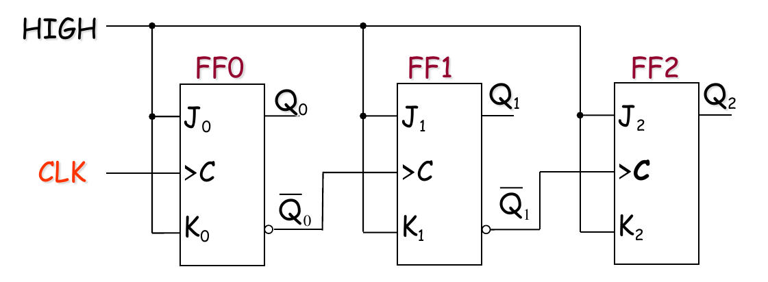
2-bit version
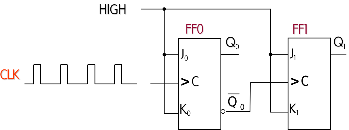
- This circuit consists of two flip-flops.
- The CLK is applied to the clock input of the first flip-flop. The second flip-flop is triggered by the output of the first flip-flop.
Timing Diagram
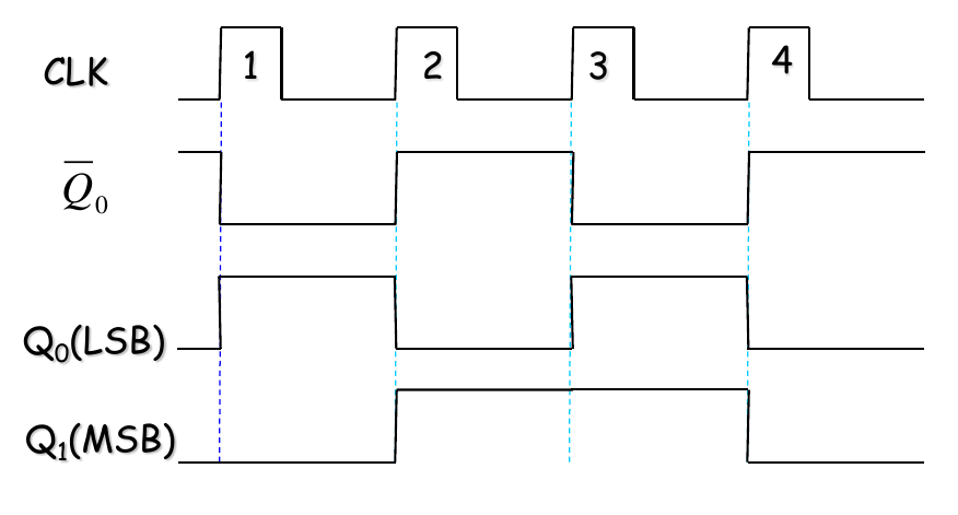
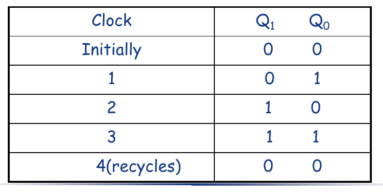
Binary state sequence
3-bit version
- 3 flip-flops
Timing Diagram
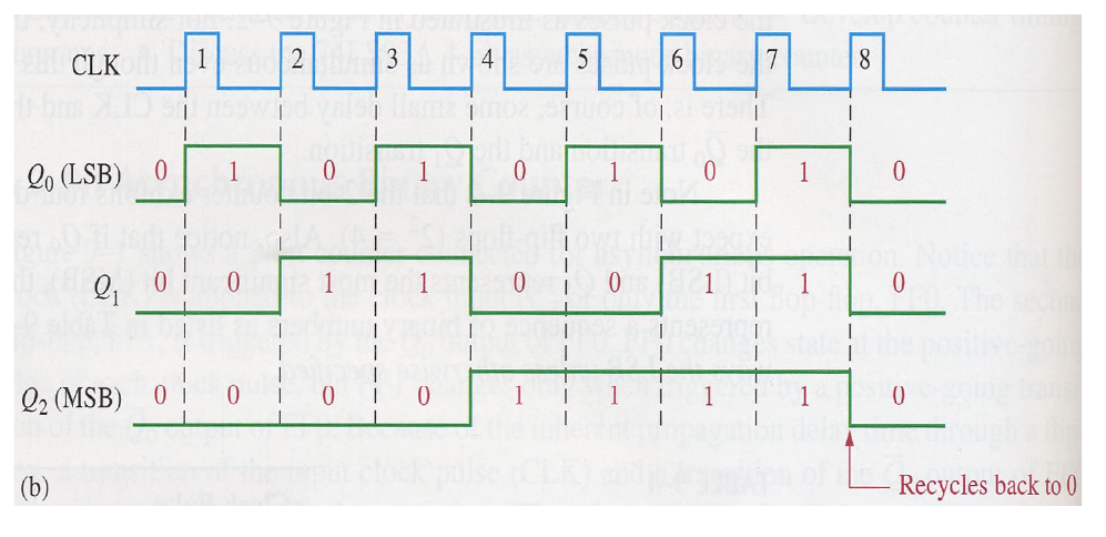
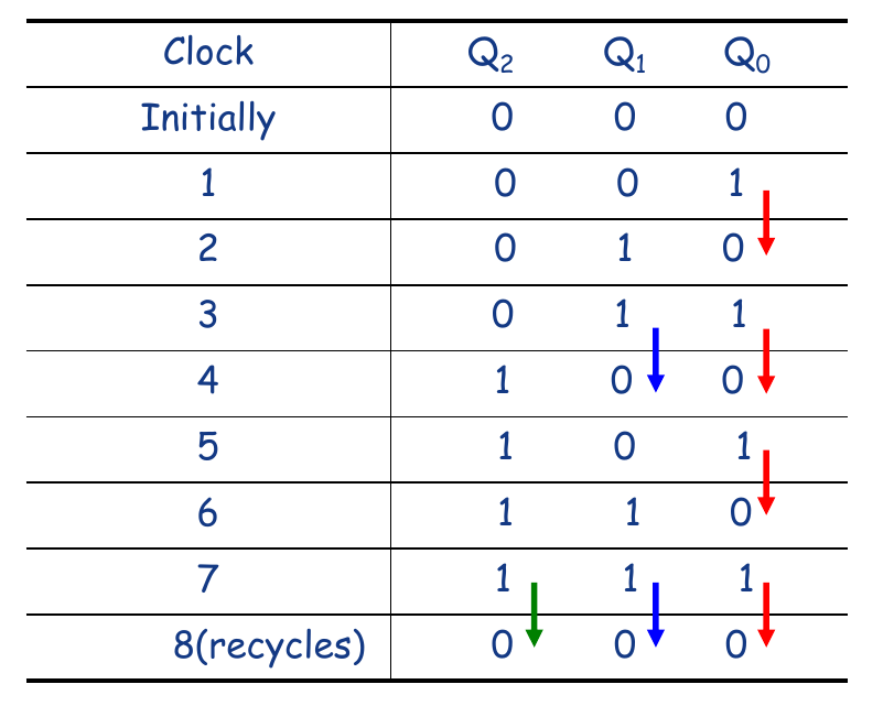
Binary state sequence
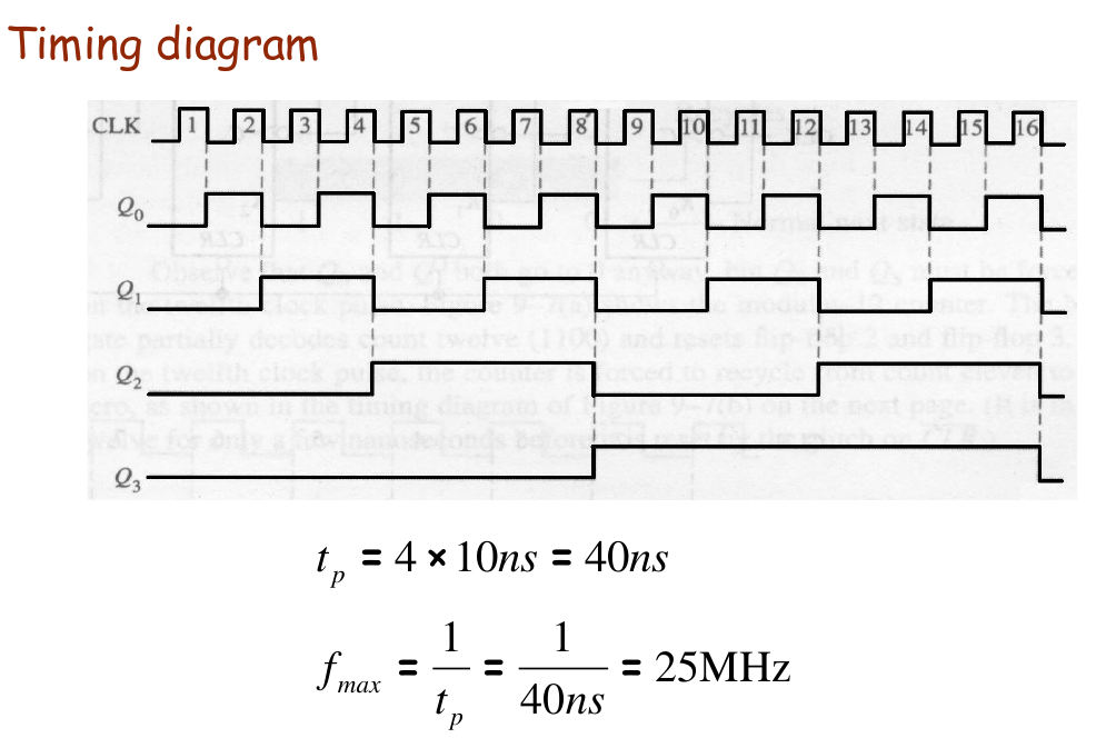
Propagation Delay
-
对于一个包含n个触发器的异步计数器,在最坏的情况下(即一个时钟脉冲导致所有触发器依次改变状态,例如从0111到1000的转换),总传播延迟 () 是所有单个触发器传播延迟之和:
- 如果所有触发器的传播延迟都相同(即 ),则总延迟为:
-
The maximum cumulative delay in a counter must be less than the period of the clock waveform.
-
总传播延迟限制了异步计数器的最高工作频率,下一个有效的时钟脉冲必须在所有触发器都稳定到新状态之后才能到达,否则会导致计数错误。
-
所以计数器最大时钟频率 () 为总传播延迟的倒数:。
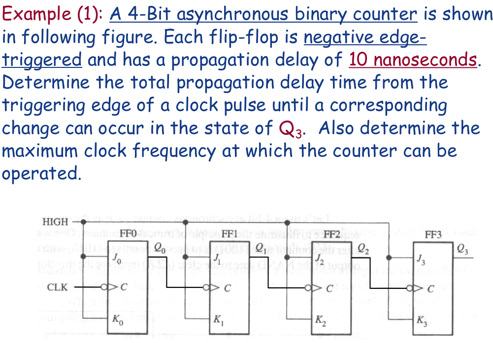
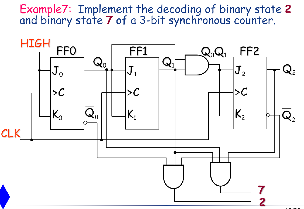
例题
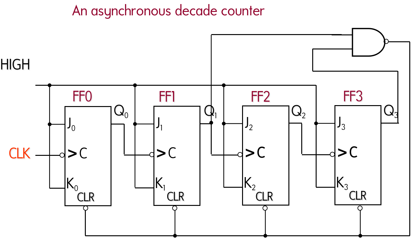
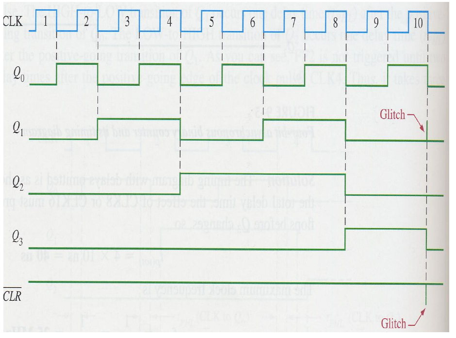
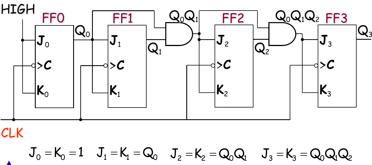
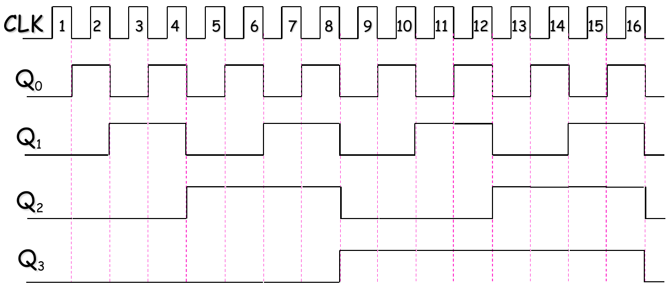
Asynchronous Decade Counter
- The modulus of a counter is the number of unique states that the counter will sequence through. The maximum possible number of states (maximum modulus) of a counter is , where is the number of flip-flops in the counter.
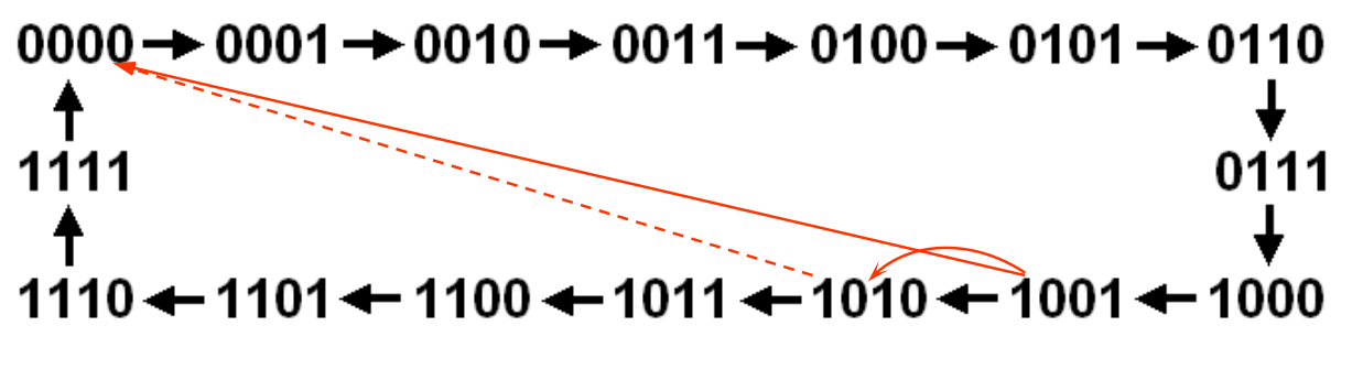
- Counters can also be designed to have a number of states in their sequence that is less than 2n. The resulting sequence is called a truncated sequence.
- One common modulus for counters with truncated sequences is ten (called MOD 10). Counters with ten states in their sequence are called decade counters. A decade counter with a count sequence of 0 through 9 is a BCD decade counter.
Method
- To obtain a truncated sequence, it is necessary to force the counter to recycle before going through all of its possible states.
- Use the Input of J-K Flip-Flops to realize this
- Be aware that there will be a glitch in the timing gram when the counter reaches 10(the output state 10 quickly pass through and then the counter is reset to 0)
MSI: A 4-Bit asynchronous binary counter (74LS93A)
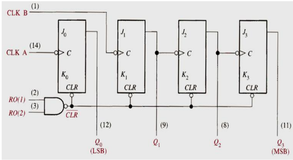
- It can be used as a divide-by-2 device if only the single FF0 is used.
- It can be used as a modulus-8 counter if only the 3-bit counter portion is used.
- It can be used as a modulus-16 counter by connecting the Q0 output to the CLK B input.
- It can be used as a decade counter by using the gated reset inputs for partial decoding of count ten (1010).
Synchoronous Counter
- The term synchronous refers to events that have a fixed time relationship with each other.
- With respect to counter operation, synchronous means that all the flip-flops in the counter are clocked at the same time by a common clock pulse.
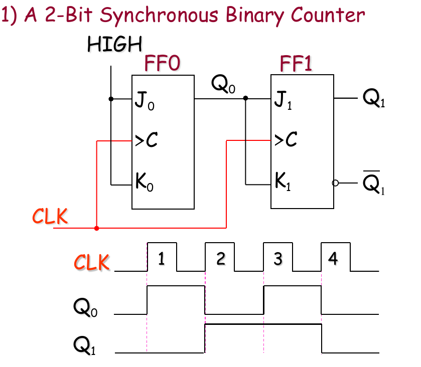
2-bit version
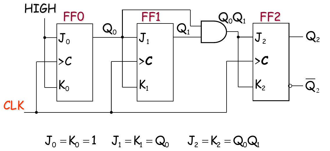
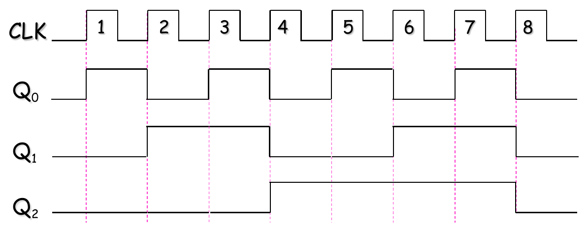
3-bit version
4-bit version
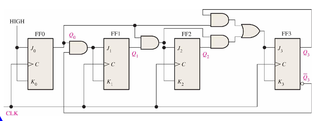
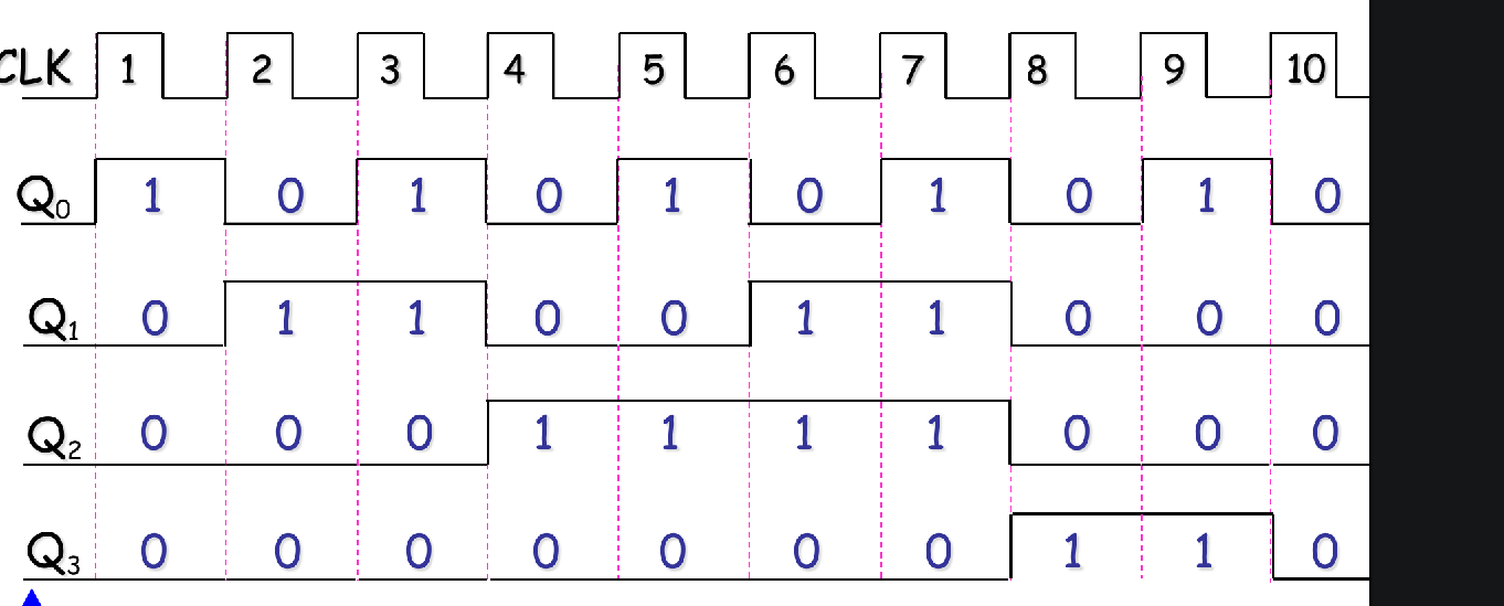
A 4-Bit Synchronous Decade Counter
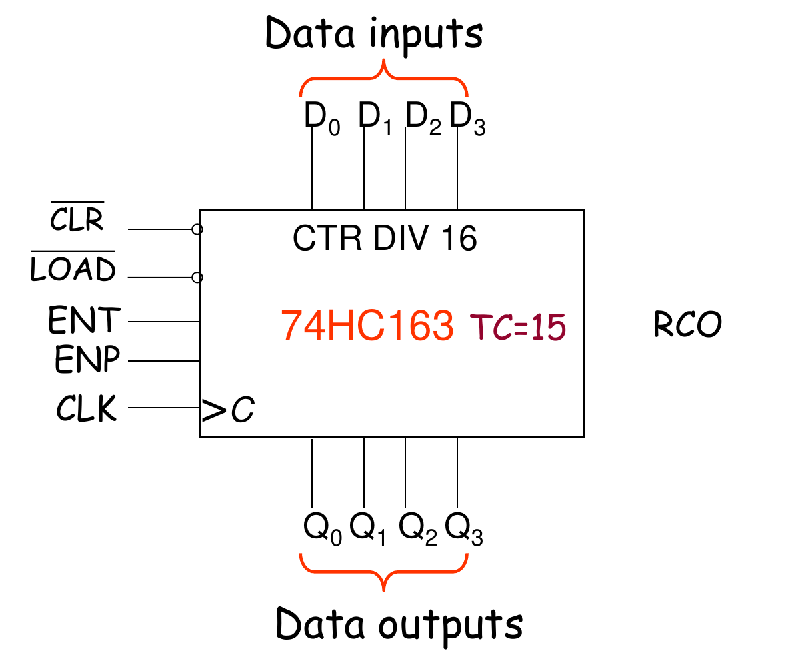
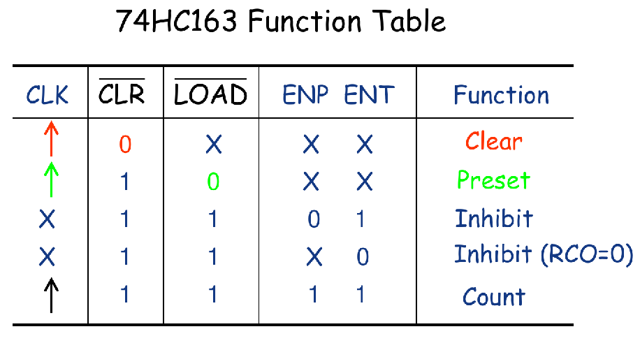
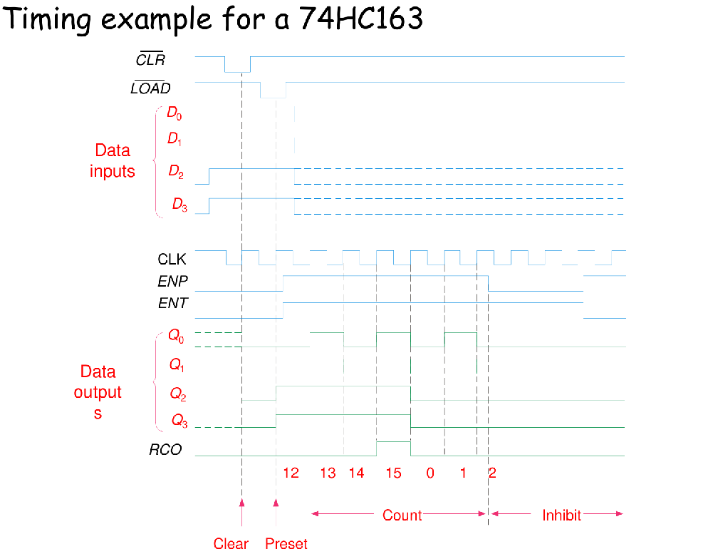
A 4-Bit Synchronous Binary Counter 74HC163
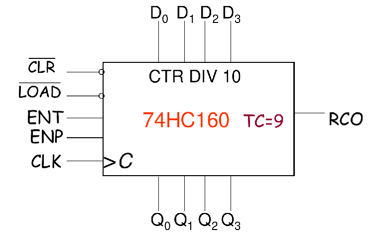
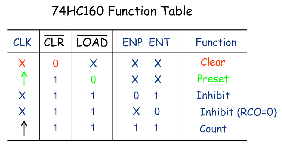
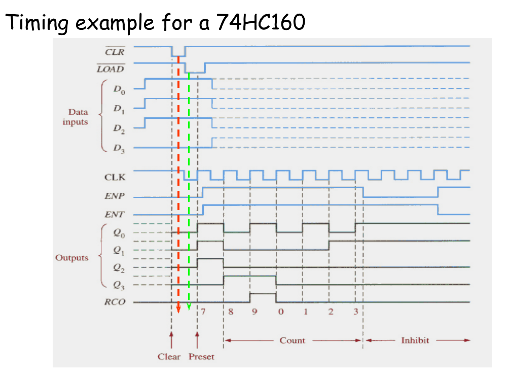
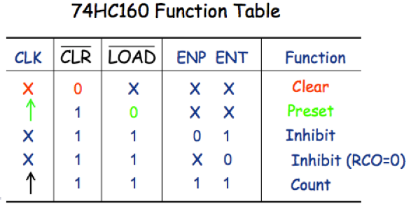
MSI: A Synchronous BCD Decade Counter 74HC160
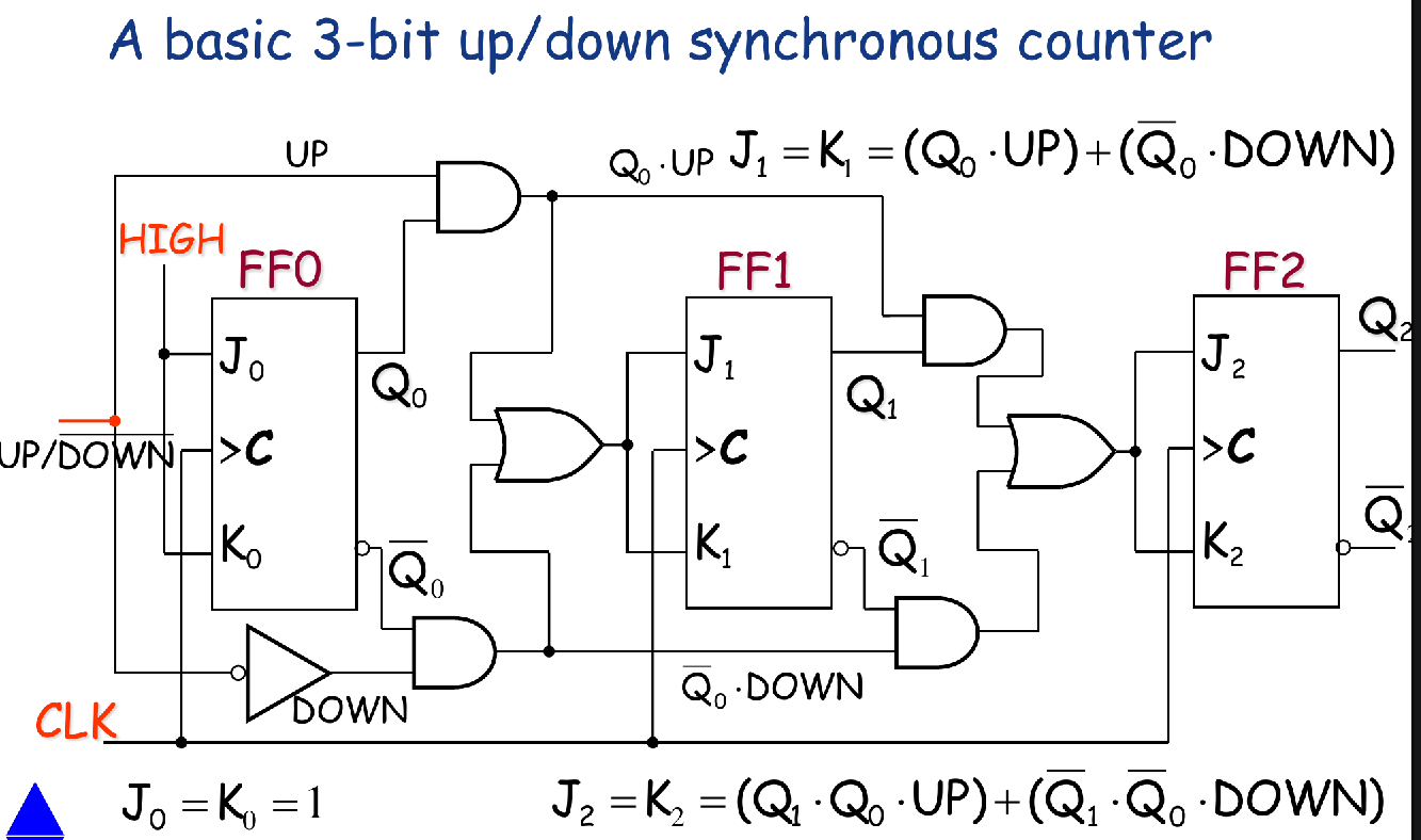
Up/Down Synchronous Counter
- An up/down counter is one that is capable of progressing in either direction through a certain sequence.
- An up/down counter, sometimes called a bidirectional counter, can have any specified sequence of states.
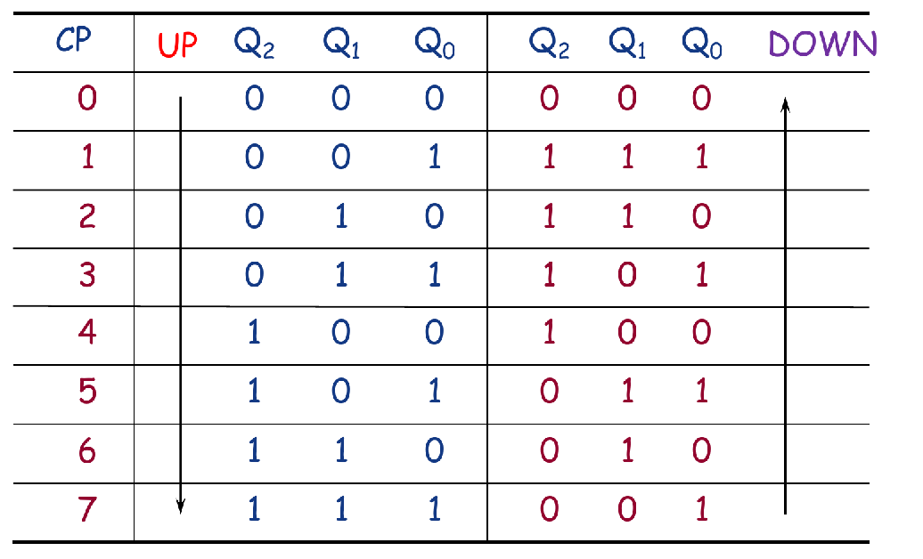
- 0,1,2,3,4,5,6,7,0,1,… UP
- 7,6,5,4,3,2,1,0,7,6,… DOWN
Up/Down sequence for a 3-bit binary counter
- For FF0:
- For FF1:
- For FF2:
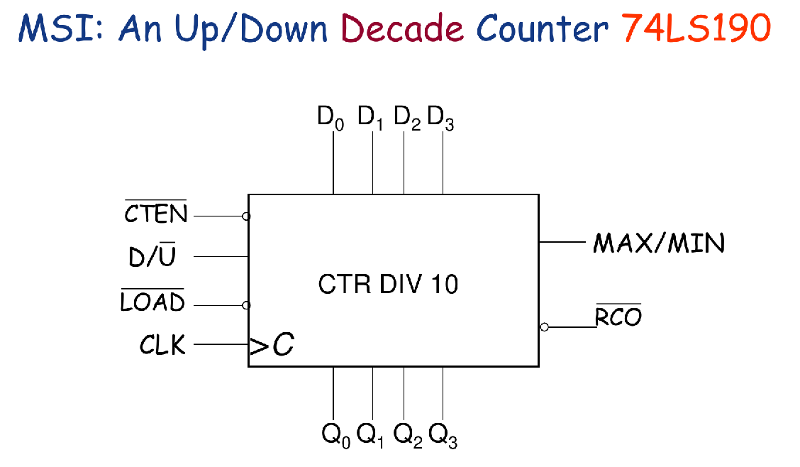
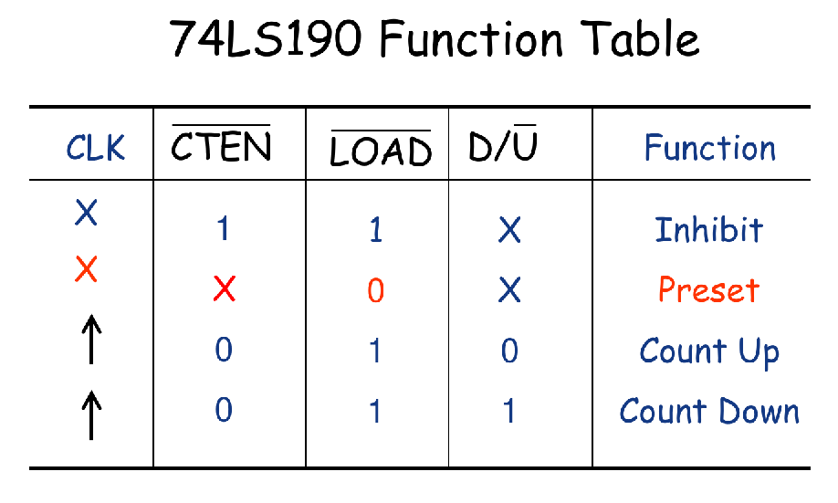
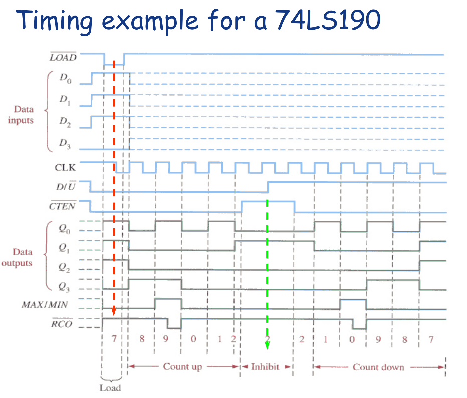
MSI: An Up/Down Decade Counter 74LS190
Design of Synchronous Counters
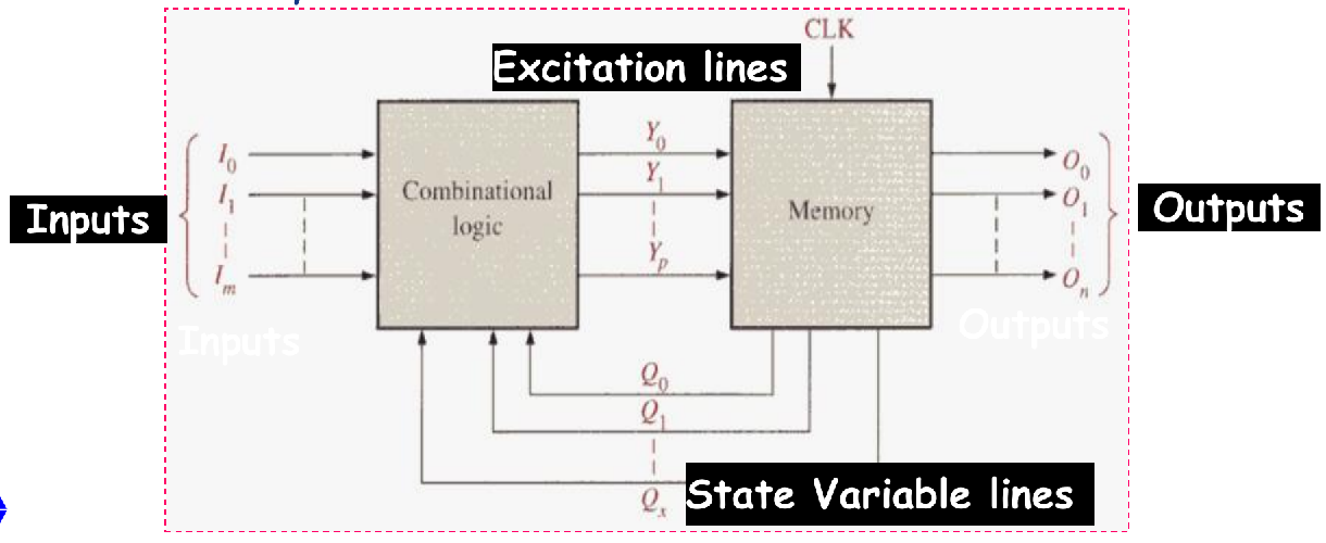
General Model of a Sequential Circuit
- A general sequential circuit consists of a combinational logic section and a memory section (flip-flops) .
- In a clocked sequential circuit, there is a clock input to the memory section.
Methods
- Develop a state diagram for a given sequence
- Develop a next-state table for a specified counter sequence.
- Create a flip-flop transition table.
- Use the Karnaugh map method to derive the logic requirements for a synchronous counter
- Implement a counter to produce a specified sequence of states.
General Design Procedure for sequential circuit
Method One
Step1: State Diagram
A counter is first described by a state diagram, which shows the progression of states through which the counter advances when it is clocked
- For an Up/Down Counter, the state diagram is bi-directional.
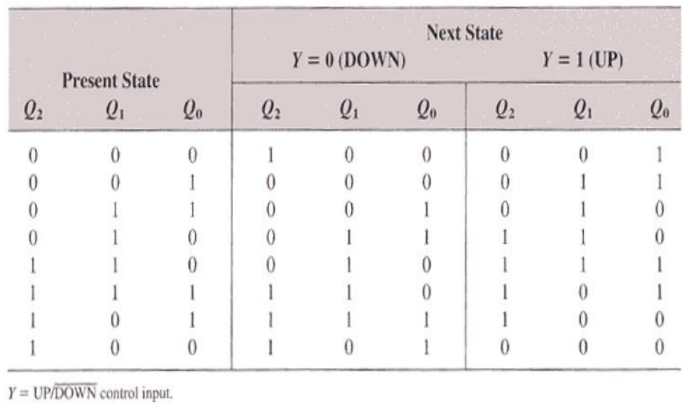
Step2: Next-State Table
The next state is the state that the counter goes to from its present state upon application of a clock pulse.
- For an Up/Down Counter, the Next-State Table has two next state section, one for up sequence, one for down sequence.
Step3: Flip-Flop Transition Table
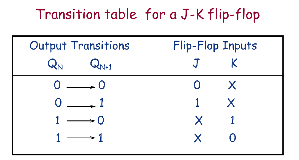
- 这个东西对于所有的JK Flip-Flop来说都是固定的,记一下很简单,大题写上去还能拿点过程分。
Step 4: Karnaugh Maps
- Karnaugh maps can be used to determine the logic required for the J and K inputs of each flip-flop in the counter.
- There is a Karnaugh map for the J input and a Karnaugh map for the K input of each flip-flop.
- In the design procedure, each cell in a Karnaugh map represents one of the present states in the counter sequence listed in next-state table.
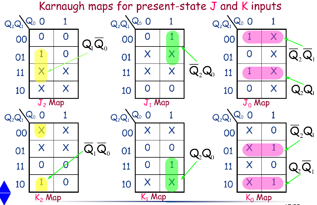
- 对于常见的4位计数器,就是8张卡诺图,每张图16个单元格
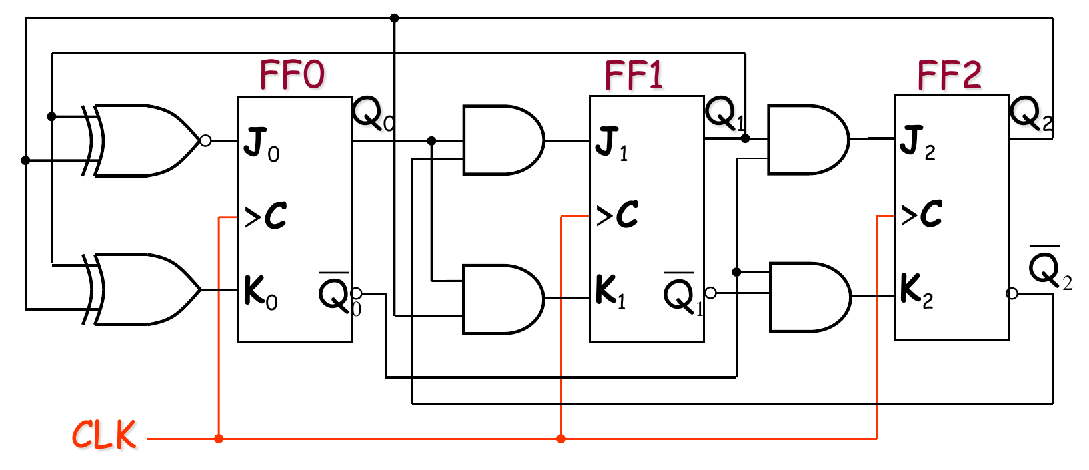
Step 5: Logic Expressions for Flip-Flop Inputs
Step 6: Counter Implementation
Summary
- Specify the counter sequence and draw a state diagram
- Derive a next-state table from the state diagram
- Develop a transition table showing the FF inputs required for each transition
- Transfer the J and K states from the transition table to Karnaugh maps which is for each input of flip-flop.
- Factor the maps to generate a logic expression for each flip-flop input.
- Implement the expressions with combinational logic, and combine with the flip-flops to create the counter.
注意事项
- 对于双向的计数器,不要忘了Next State Table和J/K的卡诺图都是要画两个方向的 UP/DOWN
Method 2
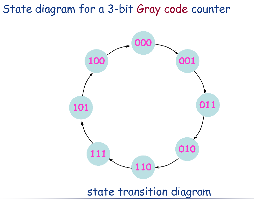
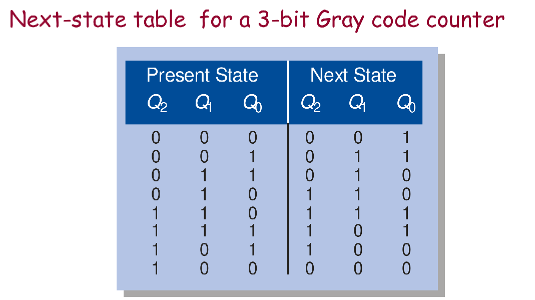
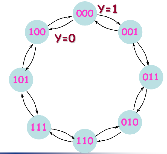
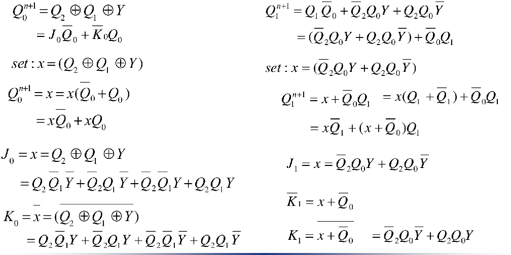
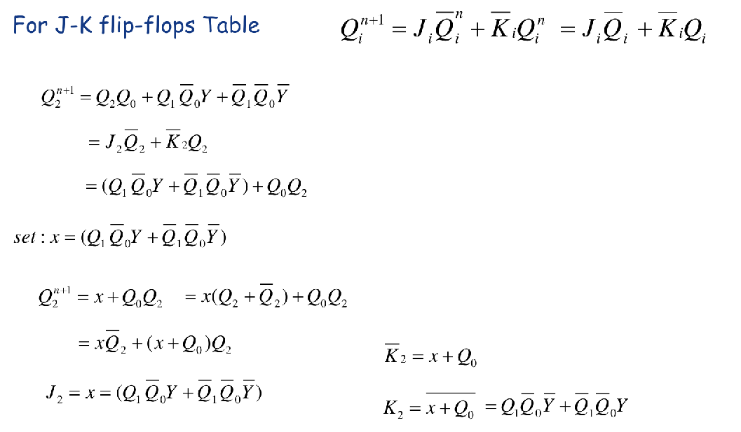
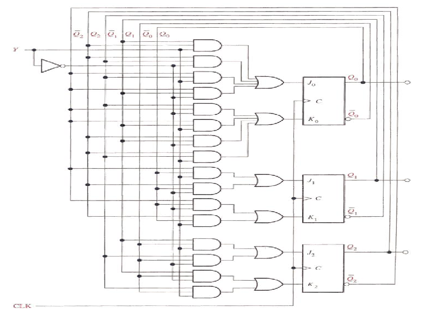
Example 8-6: Develop a synchronous 3-bit up/down counter with a Gray Code sequence. When UP/DOWN control input is 1, counter should count up. When the control input is 0, counter should count down.
Step1: State Diagram
Step 2: Next-State Table
Step 3: Karnaugh Map for next state of counter
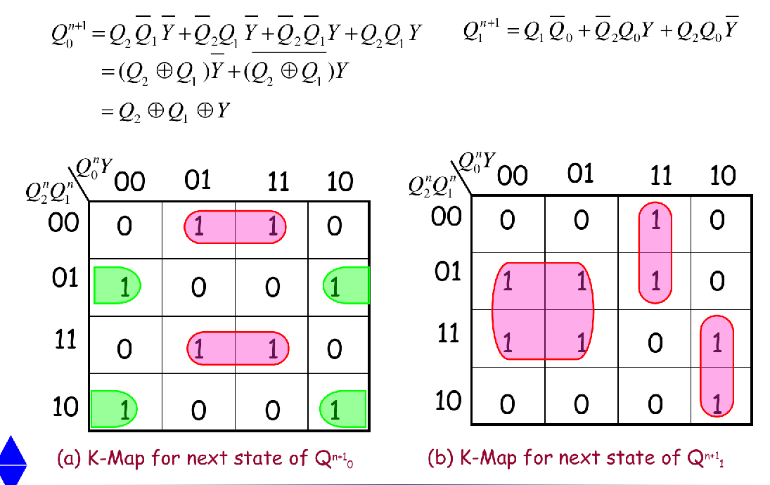
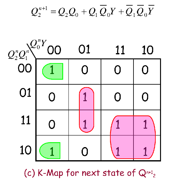
Step 4: Logic Expressions for Flip-Flop Inputs
The Logic Expression for J-K Flip-Flops is
Step 5: Counter Implementation
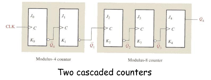
Cascaded Counters
- Counters can be connected in cascade to achieve higher-modulus operation. In essence, cascading means that the last-stage output of one counter drives the input of the next counter.
- In general, the overall modulus of cascaded counters is equal to the product of the individual modulus of all the cascaded counters.
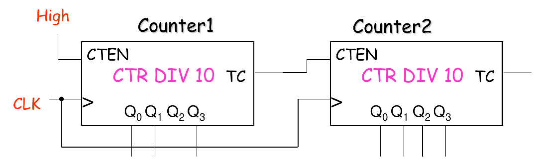
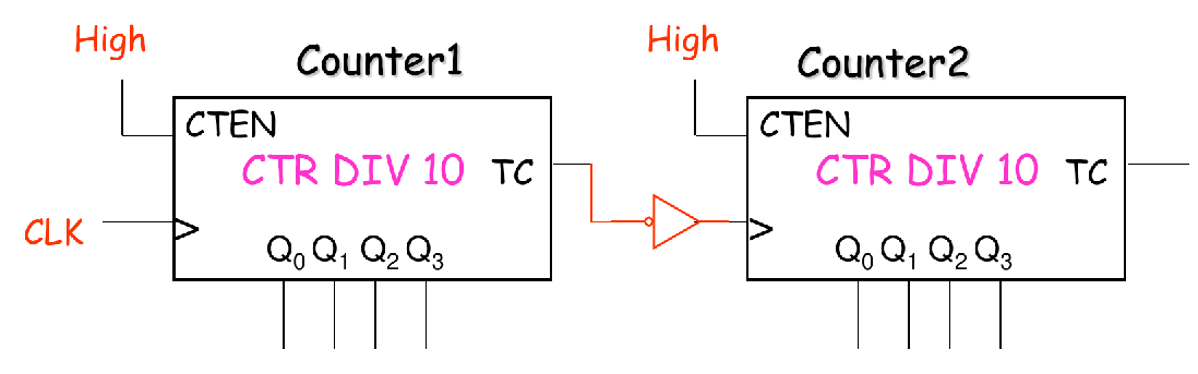
Example 1
Design a Modulus-100 Counter Using Two Cascaded Decade Counters.
方法1:TC(溢出信号)接CTEN(高一级的使能端)
方法2:TC(溢出信号)接CLK(高一级的时钟输入),CTEN置高电平
- 具体要不要接当中这个非门要看是TC是低电平有效还是高电平有效。这边TC应该是高电平有效,才要接这个非门。低电平有效的话不用接
- 总之,就是要让进位的时候(溢出的时候),高一级计数器的CLK上产生一个上升沿即可!
Frequency Divider 分频器
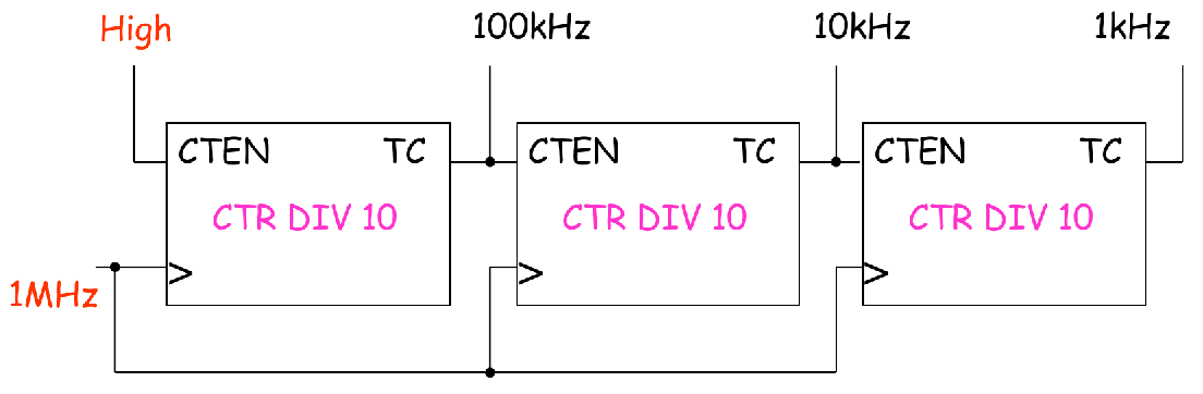
Example 2
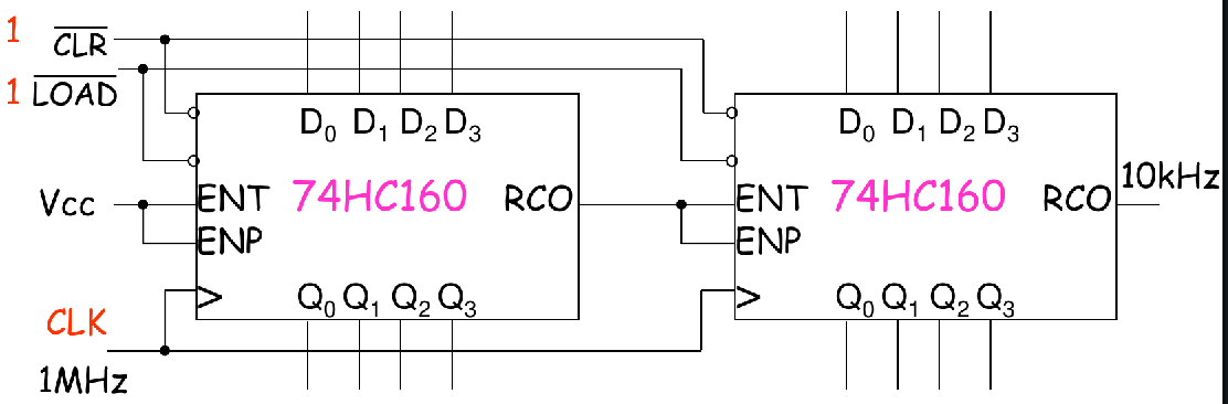
Design a divide-by-100 counter using two 74HC160
没什么花样,还是溢出接使能端
Example 3
- 关键点:注意一下CLR是异步操作,LOAD是同步操作
- 做这类题一定要看一下是同步操作还是异步操作,结果是不一样的
- 同步操作的话,应该在计数计满时触发
- 异步操作,应该在溢出时(计满的下一个数)再触发
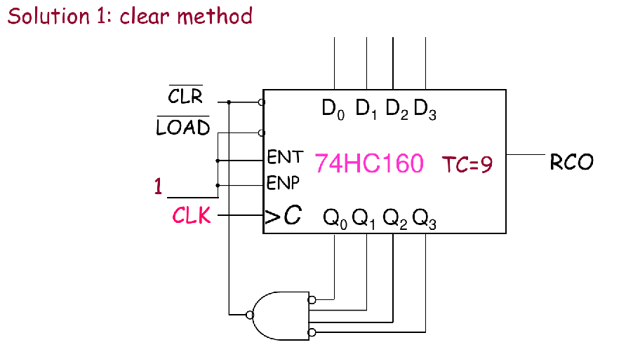
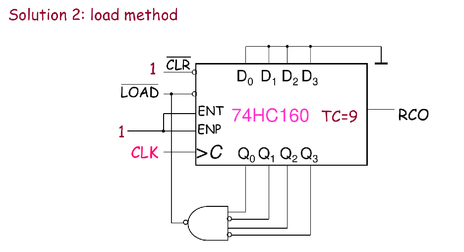
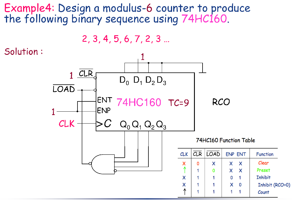
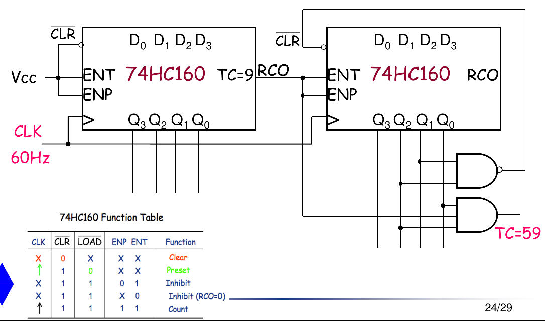
Example 4
- Sequence 不从0开始的话,那就只能用Load了!
- Sequence如果是某个值-计数器最大值(比如15),那可以不用自己接逻辑电路去判断,用RCO即可!
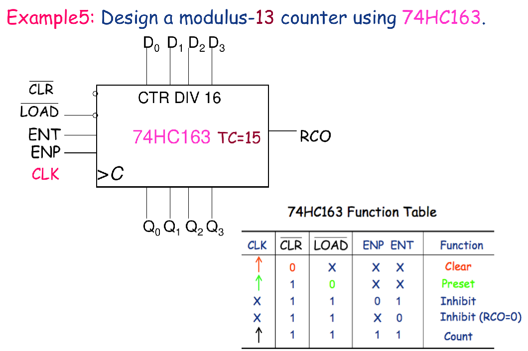
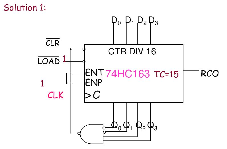
Example 5
- 关键点:还是别忘了看同步/异步操作!
- 这边Clear是同步操作哦!
Example 6: Cascaded IC Counters with Truncated Sequences
modulus-40000 counter
- 懒得写过程了,跳过
Counter Decoding
In many applications, it is necessary that some or all of the counter states be decoded. The decoding of a counter involves using decoders to determine when the circuit is in a certain state in its sequence.
没啥好说的,挺直观的
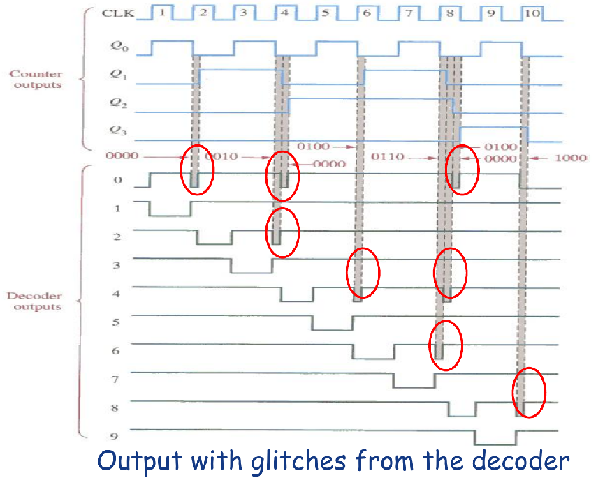
Decoding Glitches
记住两点:
- 一次计数有 个bit切换,就会有 个glitches出现
- 一般认为计数器的各个bit的切换顺序,是由低位向高位传播(低位先切,高位后切)
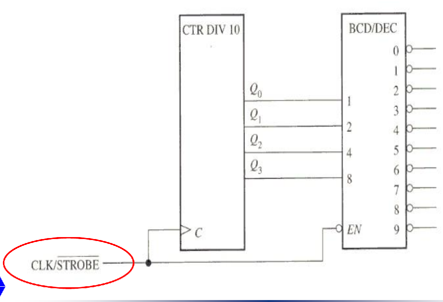
Solution: Strobing 选通
- 将CLK接到BCD解码器的,这样Decoder在CLK的低电平选通,避免了CLK上升沿的Decoding Glitches造成解码结果的抖动
- 学会画:Strobed decoder outputs for the counter
Counter Application
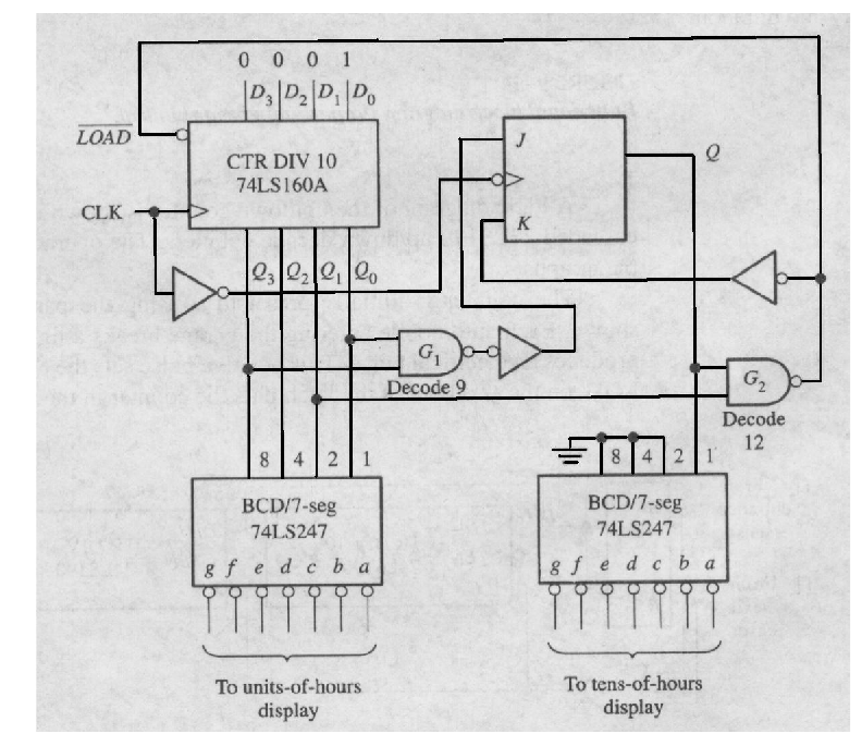
Digital Clock
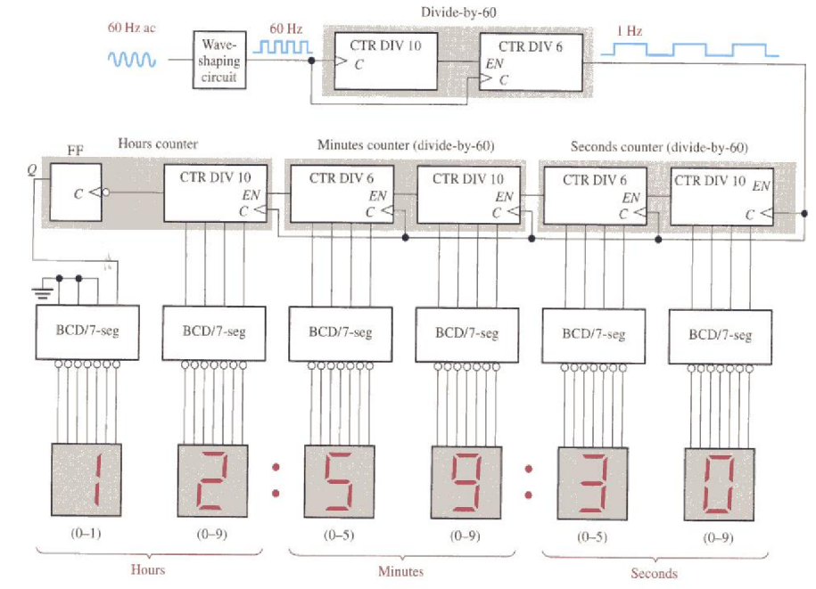
Modulus-59 Section
Hours Section